Processing method for forming pattern on the surface of optical element and apparatus thereof

A technology for optical components and processing devices, which is applied in the field of forming patterns on the surface of optical components, can solve the problems of V-shaped groove size error, influence on the quality of backlight modules, etc., and achieves the effect of short processing process and high efficiency

Inactive Publication Date: 2004-06-16
BENQ CORP
View PDF1 Cites 5 Cited by
  • Summary
  • Abstract
  • Description
  • Claims
  • Application Information

AI Technical Summary

Problems solved by technology

However, since the traditional technology uses a scraper to form multiple V-shaped grooves on the surface of the light guide plate, during the continuous scraping process, the pins are likely to cause errors in the size of the V-shaped grooves due to abrasion. In addition, for the same V As far as the groove is concerned, the force of each position of the scraping pin is not the same, and the patterns produced are also different, so it will affect the quality of the backlight module

Method used


Image

  • Processing method for forming pattern on the surface of optical element and apparatus thereof
  • Processing method for forming pattern on the surface of optical element and apparatus thereof
  • Processing method for forming pattern on the surface of optical element and apparatus thereof

Examples


Embodiment Construction

[0026] The present invention discloses a processing method for forming a pattern on the surface of an optical component by means of thermocompression, and its best embodiment and implementation method will be described in detail through the following content.

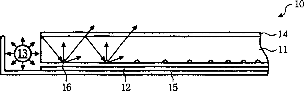
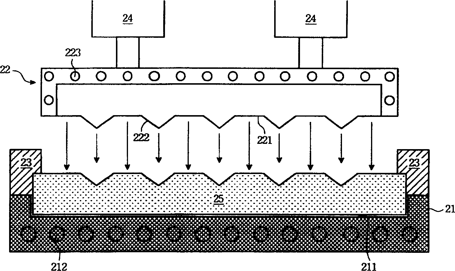
[0027] see figure 2 As shown, it is a schematic diagram of a processing device for forming patterns on the surface of an optical component of the present invention, which includes a lower mold 21 , an upper mold 22 , a clamping assembly 23 and a driving device 24 . The lower mold 21 has a bearing surface 211 , the optical component 25 is placed on the bearing surface 211 and fixed by the clamping component 23 , and a plurality of cooling pipelines 212 are arranged inside the lower mold 21 . The upper mold 22 has a pressing surface 221 corresponding to the bearing surface 211 of the lower mold 21 , and a plurality of bumps 222 with predetermined three-dimensional patterns are arranged on the surface. When the bumps 222...


PUM


Abstract

A process for forming pattern on the optical assembly surface comprising the steps of, providing a lower die, securing an optical assembly onto the bearing surface of the lower die, aligning an upper die on the top of the optical assembly, wherein a plurality of projecting spots are arranged on the compression surface of the upper die, performing thermal compression to the optical assembly by driving the upper die using a driving device, thus forcing the projecting spot on the upper die embedded into the surface of the optical assembly, and finally splitting the upper die from the optical assembly, forming patterns corresponding to the multiple projecting spots on the surface of the optical assembly.

Description

technical field [0001] The invention relates to a method for forming a pattern on the surface of an optical component, in particular to a processing method for forming a pattern on the surface of an optical component by means of thermocompression. Background technique [0002] With the rapid progress of thin-film transistor (TFT-LCD) production technology, and its advantages of thinness, power saving, and no radiation, liquid crystal displays are widely used in personal digital assistants (PDAs), notebook computers, digital cameras, Camcorders, mobile phones and other electronic products. Coupled with the industry's active investment in research and development and the adoption of large-scale production equipment, the quality of liquid crystal displays has been continuously improved, and the price has been continuously reduced, thus rapidly expanding the application field of liquid crystal displays. However, since the liquid crystal display is a non-luminescent display devi...

Claims


Application Information

Patent Timeline
Patent Type & Authority Applications(China)
IPC IPC(8): B29C43/02
Inventor 杨邦伦
Owner BENQ CORP
Why Eureka
Try Eureka