
Imbedded grating semiconductor devices

A technology of semiconductors and buried gates, which is applied in semiconductor devices, semiconductor/solid-state device manufacturing, transistors, etc., and can solve the problems of not being able to obtain conventional shutdown characteristics

Inactive Publication Date: 2004-07-07
TOYOTA JIDOSHA KK
View PDF0 Cites 5 Cited by
  • Summary
  • Abstract
  • Description
  • Claims
  • Application Information

AI Technical Summary

Problems solved by technology

However, for junction semiconductor devices, there is another problem, that is, the conventional turn-off characteristics cannot be obtained through voltage control.

Method used


Image

  • Imbedded grating semiconductor devices
  • Imbedded grating semiconductor devices
  • Imbedded grating semiconductor devices

Examples


no. 1 example

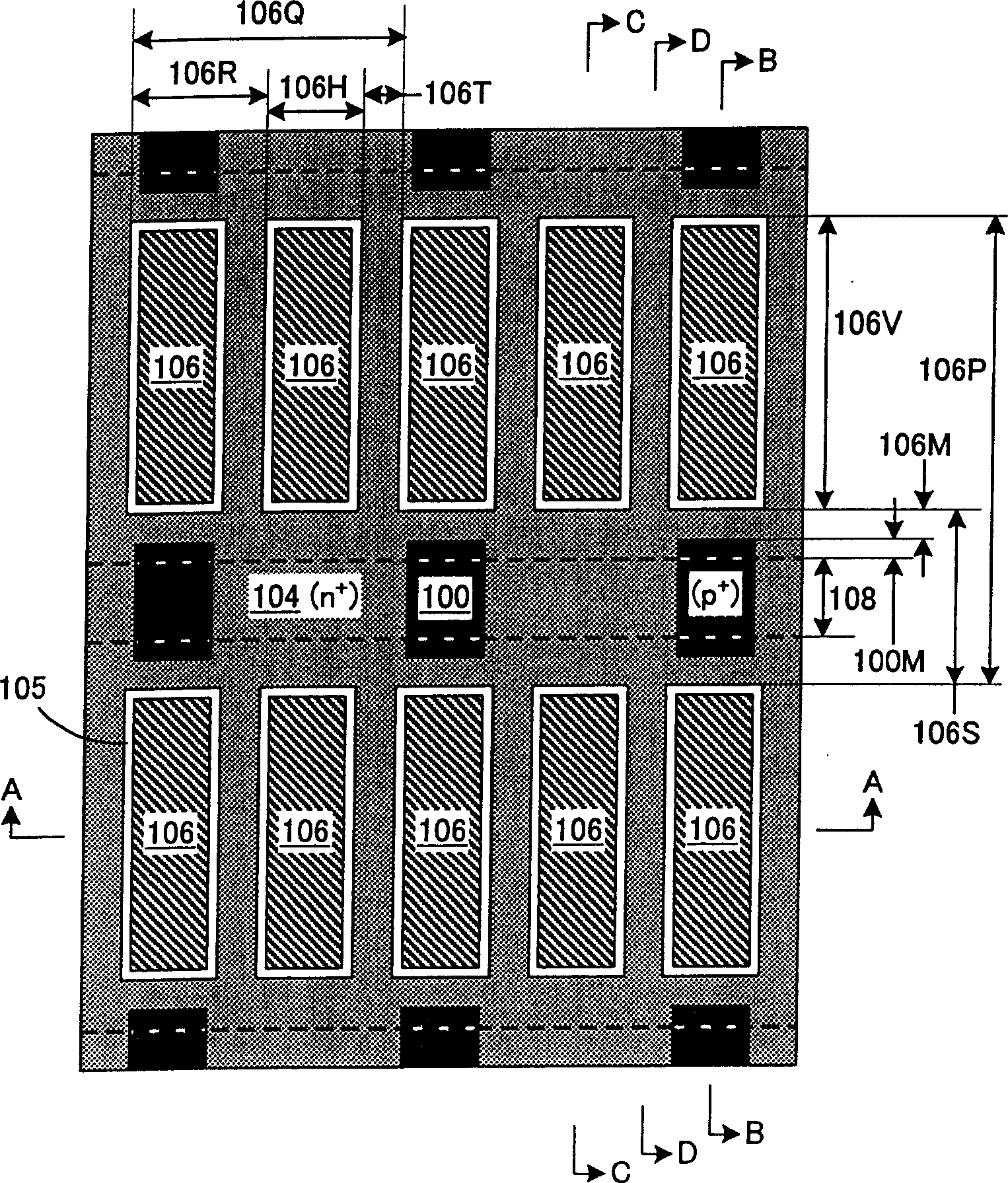
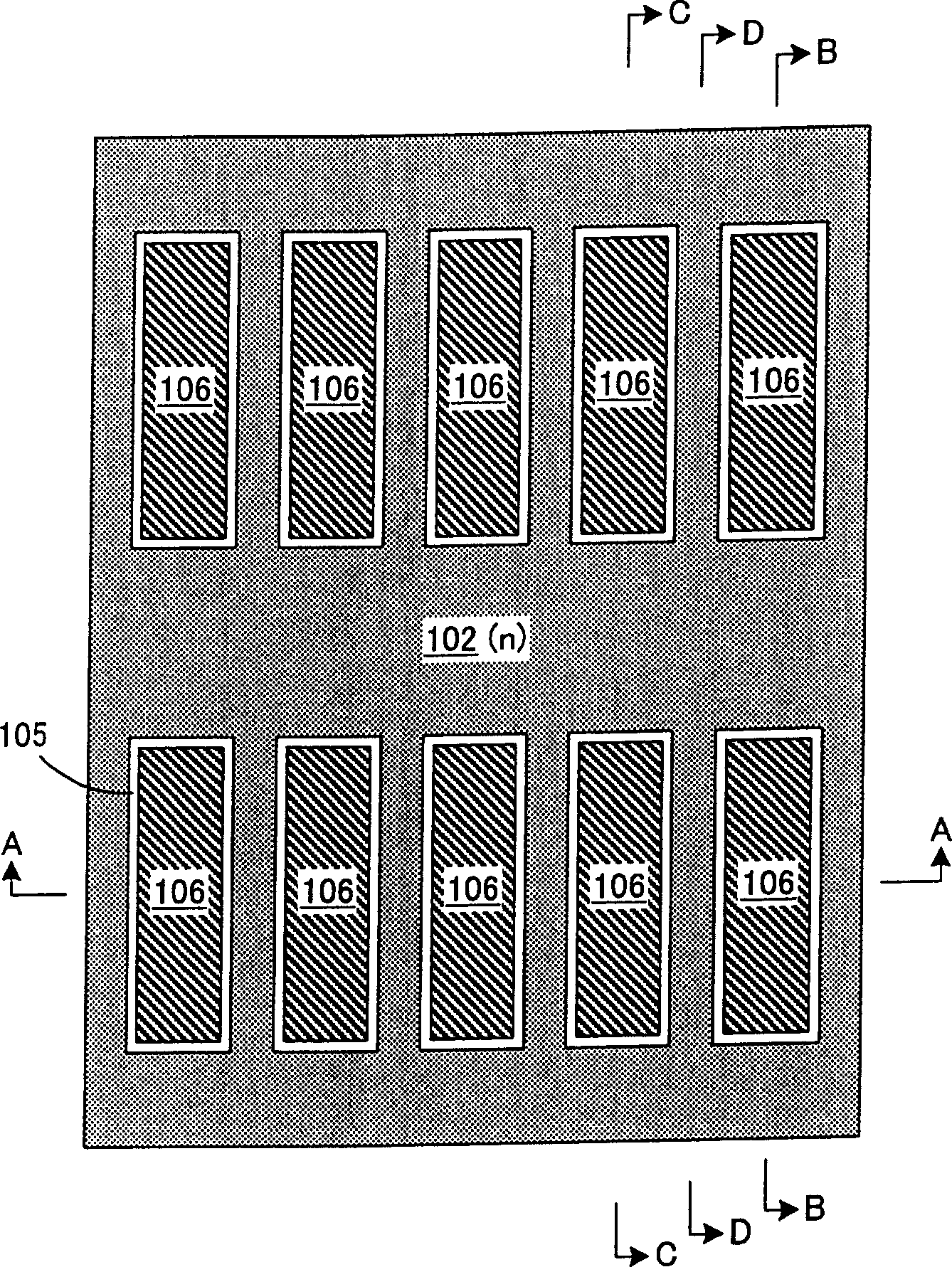
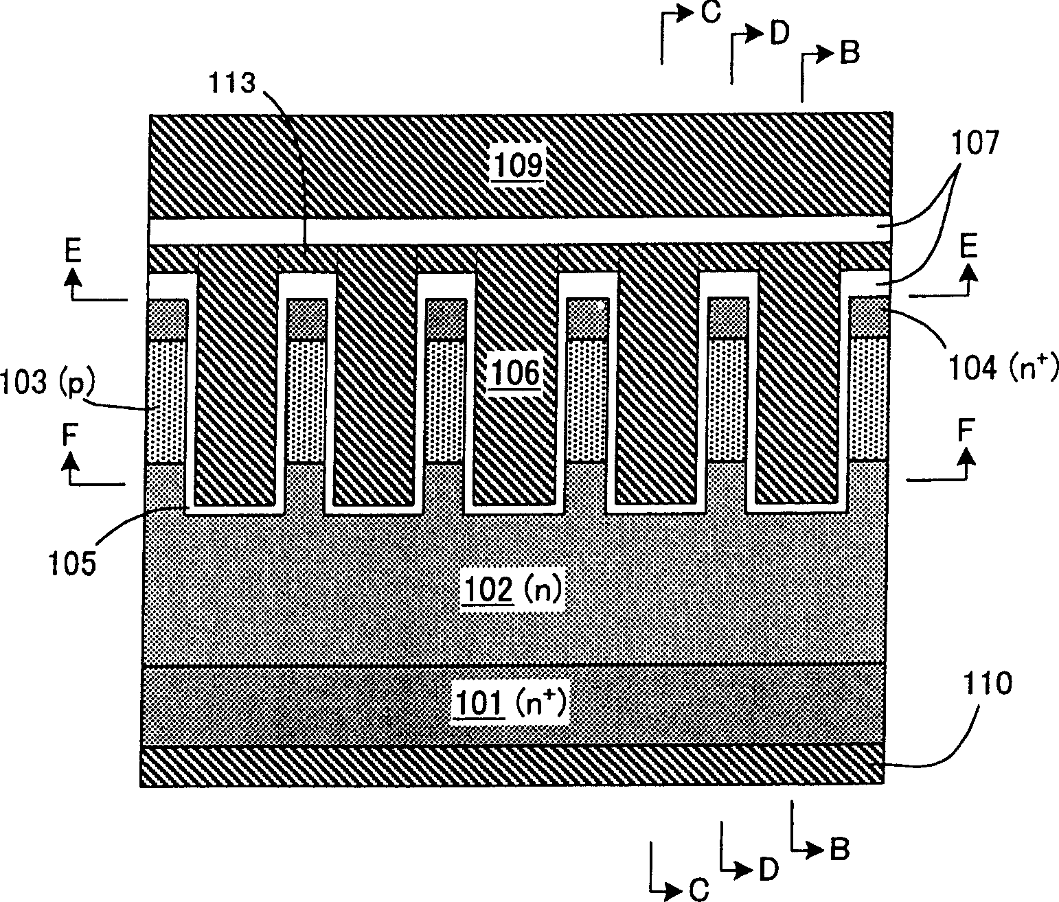
[0076] The first embodiment is a field effect type semiconductor device according to an embodiment of the present invention, having a trench type insulating gate thereon. Figure 1 to Figure 6 The structure of the field effect type semiconductor device according to the first embodiment is shown. image 3 yes figure 1 and figure 2 Sectional view of part A-A in. Figure 4 yes figure 1 and figure 2 Sectional view of part B-B in . Figure 5 yes figure 1 and figure 2 Sectional view of part C-C in . Figure 6 yes figure 1 and figure 2 Sectional view of part D-D in . figure 1 yes Figure 3 to Figure 6 A cross-sectional view of part E-E in (this plane is referred to as the "surface" of the semiconductor substrate in the specification). figure 2 yes Figure 3 to Figure 6 Cross-sectional view of part F-F in Fig.

[0077] The present field effect type semiconductor device is constructed to have a power MOS function. This field effect type semiconductor device has a st...

no. 2 example

[0101] The second embodiment is also an embodiment of the field effect type semiconductor device of the present invention, which has a trench type insulating gate. Figure 14 to Figure 17 The structure of the field effect type semiconductor device of the second embodiment is shown. Figure 15 yes Figure 14 A cross-sectional view of part B-B in the middle, while Figure 16 yes Figure 14 The cross-sectional view of part C-C in the middle. Figure 17 yes Figure 14 A cross-sectional view of part D-D in, Figure 14 yes Figure 15 to Figure 17 Cross-sectional view of part F-F in Fig. Figure 15 to Figure 17 The sectional view of the E-E part in the first embodiment is the same as that of the first embodiment figure 1 the same, where the reference numbers respectively start from "1 ** " to "2 ** ". Figure 14 The sectional view of part A-A is the same as that of the first embodiment image 3 Same, where the reference numerals are changed in the same way. In the followi...

no. 3 example

[0109] The third embodiment is also an embodiment of the field effect type semiconductor device of the present invention, which has a trench type insulated gate. Figure 22 to Figure 27 The structure of the field effect type semiconductor device of the third embodiment is shown. Figure 24 is Figure 22 and Figure 23 The cross-sectional view of part A-A in . Figure 25 is Figure 22 and Figure 23 A cross-sectional view of part B-B in the middle, while Figure 26 yes Figure 22 and Figure 23 The cross-sectional view of part C-C in the middle. Figure 27 yes Figure 22 and Figure 23 Sectional view of part D-D in . Figure 22 is Figure 24 to Figure 27 The cross-sectional view of part E-E in, Figure 23 is Figure 24 to Figure 27 Cross-sectional view of part F-F in Fig.

[0110] Like the first and second embodiments, the present field effect type semiconductor device is composed to perform the Power MOS function. In terms of structure, this embodiment has the sam...


PUM


Abstract

An object of this invention is to provide a buried gate-type semiconductor device in which the interval between adjacent buried gate is minimized so as to improve channel concentration thereby realizing low ON-resistance. Voltage-resistance reduction due to the concentration of electrical fields in the vicinity of the bottom of the gates is prevented and good OFF characteristics are achieved at the same time by means of P<+> body regions deeper than the bottom portion of the buried gates. A plurality of gate electrodes (106) each having a rectangular section are disposed in the plan of a substrate. The interval (106T) between the long sides of the gate electrodes (106) is made shorter than the interval (106S) between the short sides thereof. Further, a belt-like contact opening (108) is provided between the short sides of the gate electrode (106), so that P<+> body regions (100) and N<+> source region (104) are in contact with a source electrode. Consequently, the interval (106T) between the long sides of the gate electrode (106) can be set up regardless of the width of the contact opening (108).

Description

technical field [0001] The present invention relates to a semiconductor device provided with a buried gate. More specifically, it relates to a buried gate type semiconductor device whose inter-gate spacing is as short as possible so as to increase the channel concentration and reduce on-resistance, and to a buried gate type semiconductor device which aims to be able to A decrease in withstand voltage due to local electric field concentration around the gate bottom is prevented. In particular, the buried gate type semiconductor device of the present invention is effective for high withstand voltage power semiconductor devices. Background technique [0002] Conventionally, a buried gate type semiconductor device is used to supply power and the like (for example, an insulated gate type bipolar transistor disclosed in JP Laid-Open Patent Publication No. 2002-100770). Some such conventional buried gate type semiconductors are striped in which the striped buried gates are arrang...

Claims


Application Information

Patent Timeline
Patent Type & Authority Applications(China)
IPC IPC(8): H01L29/80H01L21/331H01L21/336H01L29/06H01L29/08H01L29/10H01L29/423H01L29/739H01L29/78
CPCH01L29/0878H01L29/7813H01L29/4236H01L29/7722H01L29/7397H01L29/7392H01L29/66348H01L29/1095H01L29/0696H01L29/4238H01L29/7828
Inventor 栉田知义
Owner TOYOTA JIDOSHA KK
Learn More