Channel structure of high voltage NMOS field transistor in EEPROM peripheral circuit and manufacturing method thereof

A channel structure and peripheral circuit technology, applied in the manufacture of circuits, electrical solid devices, semiconductor/solid devices, etc., can solve the problems of increasing process cost, reducing isolation size, increasing lithography, etc., to save process cost and reduce isolation size, the effect of increasing the threshold voltage

Inactive Publication Date: 2008-01-23
SHANGHAI HUA HONG NEC ELECTRONICS
View PDF0 Cites 2 Cited by
  • Summary
  • Abstract
  • Description
  • Claims
  • Application Information

AI Technical Summary

Problems solved by technology

Since the doping concentration of the N well of the memory cell is not high, in order to reduce the isolation size, a field ion implantation is usually performed under the field oxide layer, which requires an additional photolithography and increases the process cost.

Method used


Image

  • Channel structure of high voltage NMOS field transistor in EEPROM peripheral circuit and manufacturing method thereof
  • Channel structure of high voltage NMOS field transistor in EEPROM peripheral circuit and manufacturing method thereof
  • Channel structure of high voltage NMOS field transistor in EEPROM peripheral circuit and manufacturing method thereof

Examples


Embodiment Construction

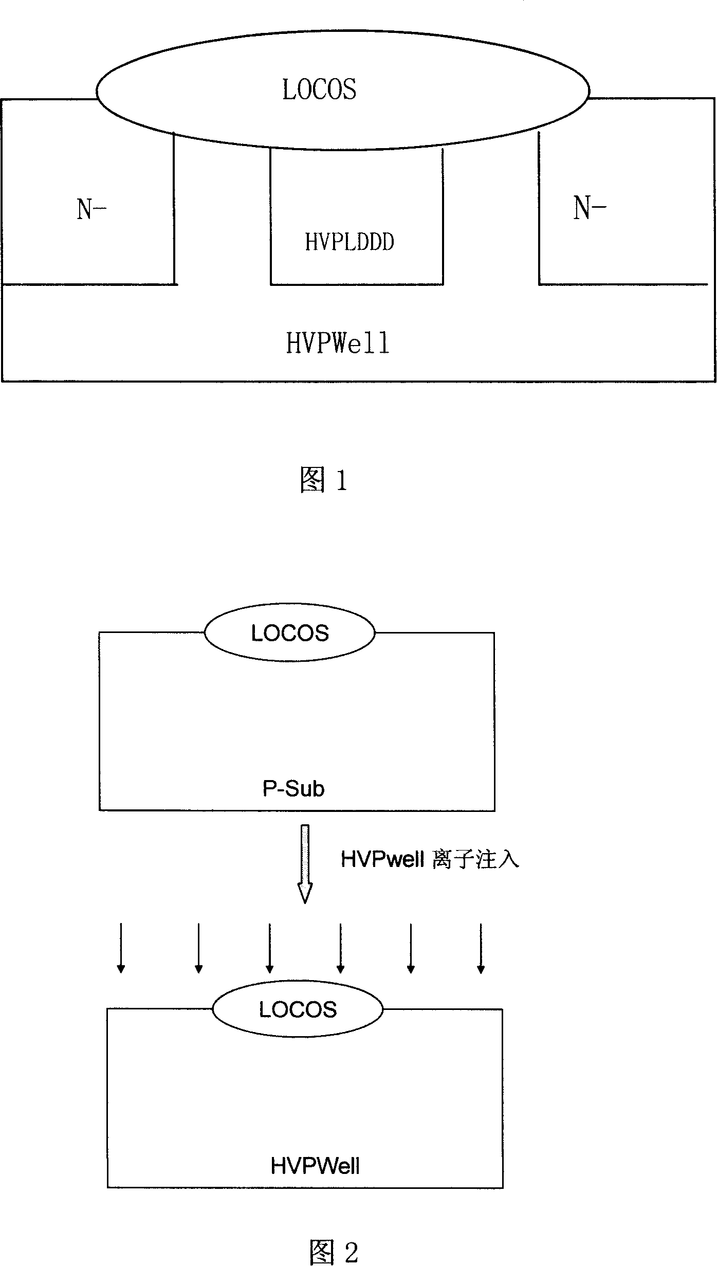
[0011] Since the doping concentration of the transistor channel of the EEPROM cell is usually relatively low, the isolation between the cells is difficult. A sufficiently high threshold voltage Vt2.

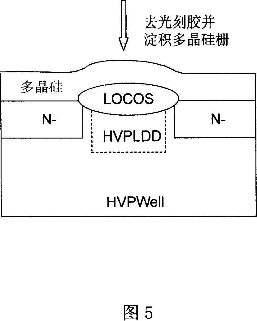
[0012] The channel structure of the high-voltage NMOS field transistor in the EEPROM peripheral circuit of the present invention is shown in Figure 1. On the high-voltage P-well (HV PWell), two lightly doped source-drain N-type N-regions of unit tubes are formed, and in the N-region Boron ions are implanted in the channel between them, and at the same time, the N-region and the channel are isolated by local silicon oxide (LOCOS). A structure in which a field implantation region is embedded in the channel of the field effect transistor is formed.

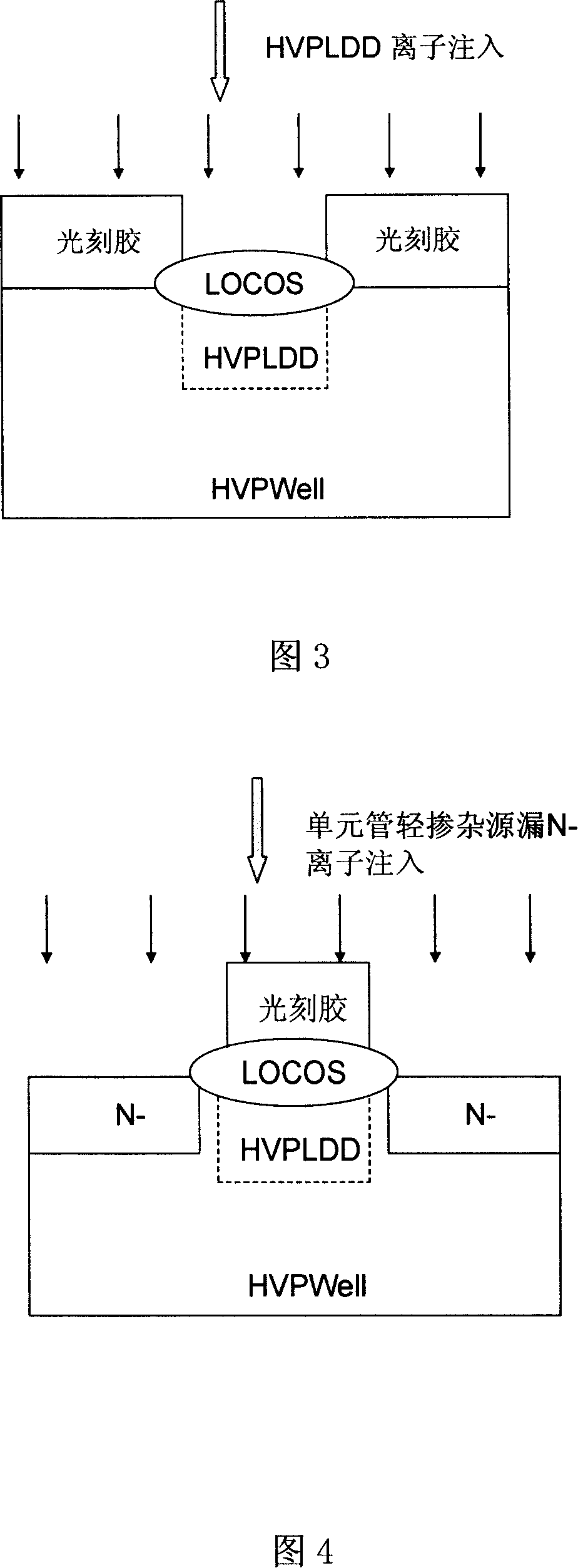
[0013] The manufacturing process flow of the high-voltage NMOS field transistor that realizes the above channel structure is:

[0014] On a P-type substrate (P-Sub) with LOCOS isolation, HV Pwell ion implantation is performed to form ...


PUM


Abstract

The present invention discloses a trench structure for medium and high voltage NMOS field transistor of EEPROM peripheral circuit, which is filled with boron ions. Production technique of the trench structure lies in that in current technical flows, a trench area is opened through photo-etching. In synchronization with light dope / boron implantation into high-voltage PMOS transistor, boron ions are implanted into the trench. The present invention ensures more effective field isolation, reduces unit area and improves chip integration.

Description

technical field [0001] The invention relates to a channel structure of a high-voltage NMOS (N-type metal oxide semiconductor) field transistor (Field Transistor) in an EEPROM peripheral circuit; the invention also relates to a manufacturing process method of the channel structure. Background technique [0002] With the increasing development of semiconductor manufacturing technology, the competition in integrated circuit design has become increasingly fierce, especially in the design of memory cells, in order to improve competitiveness, it is necessary to reduce the cell area as much as possible and simplify the manufacturing process. In a memory cell, a large area is used for isolation between cells. If the isolation distance between cells can be shortened, the cell area will be effectively reduced. [0003] In EEPROM (Electrically Erasable Programmable Read-Only Memory) cells, the size of the cells turns out to be smaller, so the isolation size is also required to be small...

Claims


Application Information

Patent Timeline
Patent Type & Authority Applications(China)
IPC IPC(8): H01L29/78H01L27/115H01L21/336H01L21/265H01L21/8247
Inventor 钱文生
Owner SHANGHAI HUA HONG NEC ELECTRONICS
Why Eureka
Try Eureka