Pixel structure

A pixel structure, pixel technology, applied in optics, instruments, electrical components, etc., can solve problems such as failure, complicated driving circuit design and manufacturing, and pixel structure cannot operate normally, and achieve the effect of uniform electric field distribution and simplified design.

Inactive Publication Date: 2004-07-28
AU OPTRONICS CORP
View PDF0 Cites 7 Cited by
  • Summary
  • Abstract
  • Description
  • Claims
  • Application Information

AI Technical Summary

Problems solved by technology

Therefore, the design of this pixel structure is susceptible to failure due to the influence of pollution particles in the manufacturing process, that is, if there are pollution particles attached to a certain part of the pixel structure and cause defects such as short circuits, it may cause the entire pixel structure to malfunction. operate
Moreover, the existing pixel storage capacitor 120 adopts a structure configured on the scanning wiring 101a, so that the design and manufacture of the driving circuit will be more complicated because the scanning waveform needs to be designed one more level.

Method used


Image

  • Pixel structure
  • Pixel structure
  • Pixel structure

Examples


no. 1 example

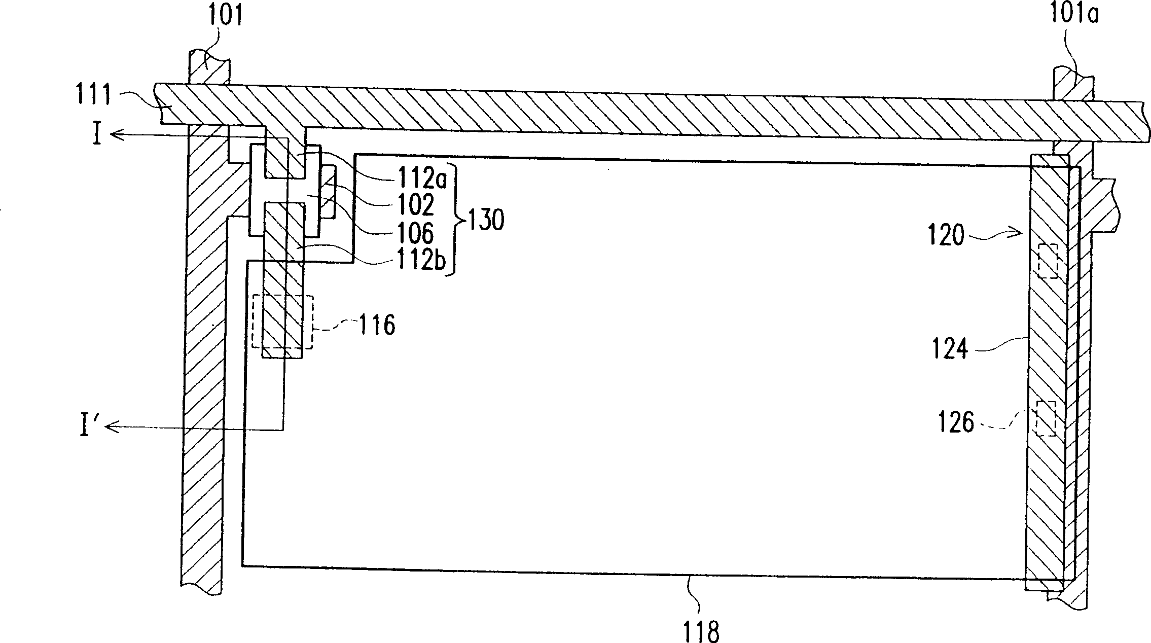
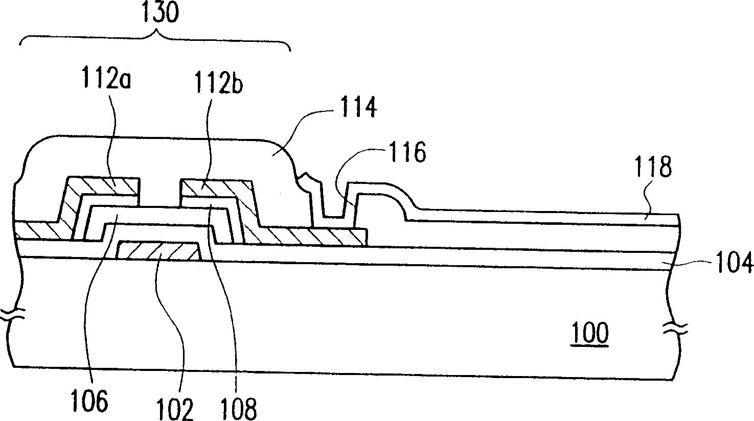
[0024] Such as image 3 , which shows a top view of a pixel structure according to a preferred embodiment of the present invention; and Figure 4 shown as image 3 The schematic diagram of the II-II' section in .

[0025] Please refer to image 3 and Figure 4 , the manufacturing method of the pixel structure of the present invention first provides a substrate 200, wherein the substrate 200 is, for example, a transparent glass substrate or a transparent plastic substrate. Next, a scan line 201 and a gate 202 are formed on the substrate 200 , wherein the scan line 201 is electrically connected to the gate 202 .

[0026] Afterwards, a gate dielectric layer 204 is completely formed on the substrate 200 to cover the scan lines 201 and the gates 202 . The material of the gate dielectric layer 204 is, for example, a dielectric material such as silicon nitride or silicon oxide.

[0027] Next, a channel layer 206 is formed on the gate dielectric layer 204 above the gate 202, whe...

no. 2 example

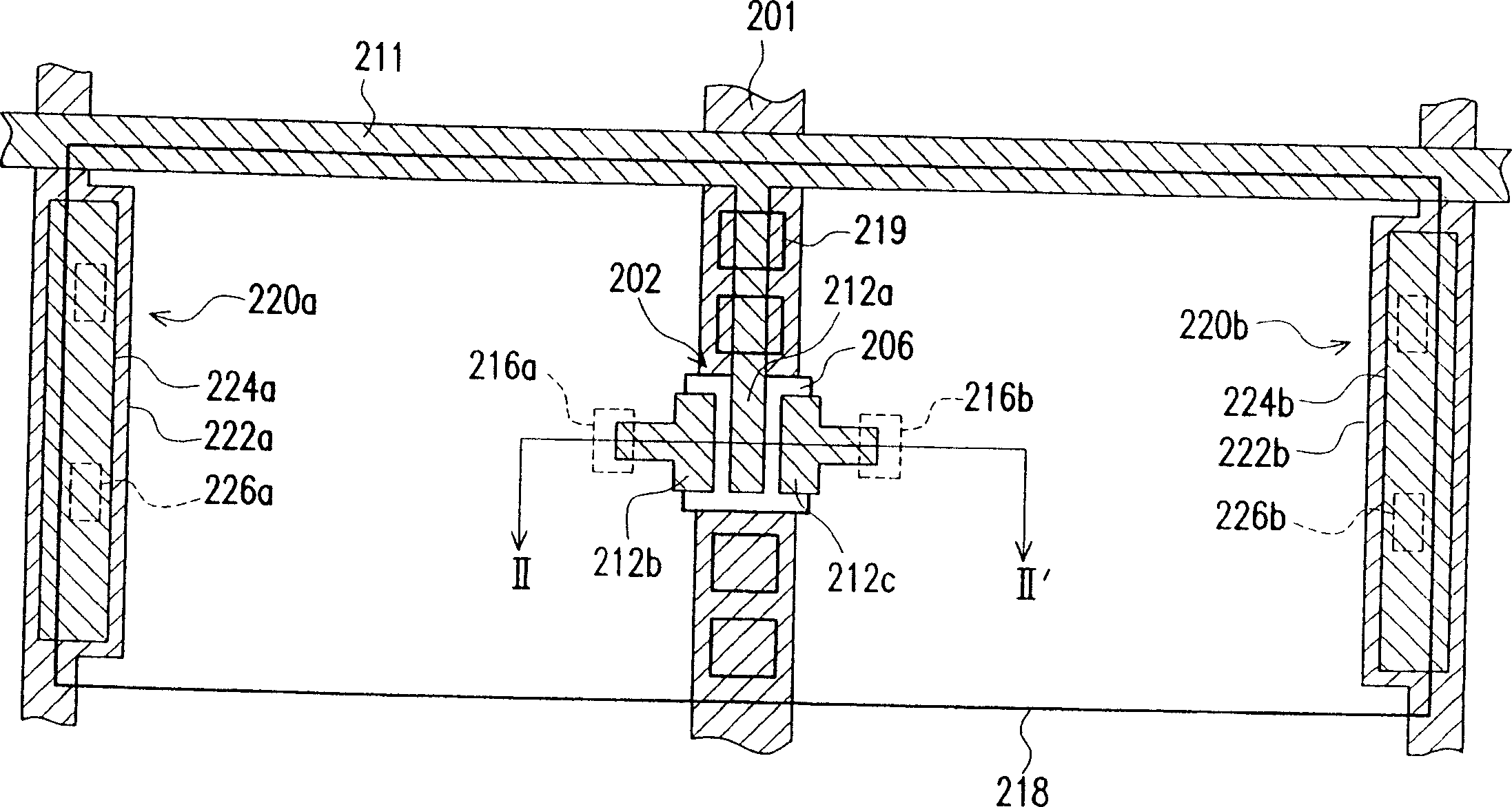
[0038] Figure 5 Shown is a top view of a pixel structure according to another preferred embodiment of the present invention; Figure 7 shown as Figure 5 The schematic diagram of the III-III' section.

[0039] Please refer to Figure 5 and Figure 7 The manufacturing method of the pixel structure in this embodiment is to firstly provide a substrate 300, wherein the substrate 300 is, for example, a transparent glass substrate or a transparent plastic substrate. Next, a scan line 301 and a gate 302 are formed on the substrate 300 , wherein the scan line 301 is electrically connected to the gate 302 .

[0040] Afterwards, a gate dielectric layer 304 is completely formed on the substrate 300 to cover the scan lines 301 and the gates 302 . The material of the gate dielectric layer 304 is, for example, a dielectric material such as silicon nitride or silicon oxide.

[0041] Next, a channel layer 306 is formed on the gate dielectric layer 304 above the gate 302 , wherein the m...


PUM


Abstract

The present invention relates to a pixel structure, it is suitable for framing on a base plate. It includes a scan line distributed on the base plate; a grid dielectric layer laid on the base plate and used for covering the scan line; a data line laid on the guide dielectric layer, and the extended direction of the data line is different from the extended direction of scan line; a protective layer laid on the grid dielectric layer and used for covering the data line; a transparent pixel electrode laid on protective layer and a double-drain film transistor placed on the base plate, in which the double-drain film transistor has a grid, a channel layer, a source and two drains, the source is connected with data line, two drains are respectively electrically connected with transparent pixel electrode, and the grid is electrically connected with scan line.

Description

technical field [0001] The invention relates to a structure of a semiconductor element, in particular to a pixel structure of a thin film transistor liquid crystal display (Thin Film Transistor Liquid Crystal Display, TFT-LCD). Background technique [0002] TFT-LCD is mainly composed of a thin-film transistor array substrate, a color filter array substrate and a liquid crystal layer, wherein the thin-film transistor array substrate is composed of a plurality of pixel structures arranged in an array, which includes a plurality of thin-film Transistors / thin film transistors and a pixel electrode corresponding to each thin film transistor. The thin film transistor includes a gate / gate, a channel layer / channel layer, a drain and a source, and the thin film transistor is used as a switch component of a liquid crystal display unit. [0003] Such as figure 1 , which shows a schematic top view of an existing pixel structure; figure 2 for figure 1 The I-I' cross-sectional schema...

Claims


Application Information

Patent Timeline
Patent Type & Authority Applications(China)
IPC IPC(8): G02F1/1343G02F1/136H01L21/3205
Inventor 吕安序
Owner AU OPTRONICS CORP
Why Eureka
Try Eureka