Active matrix liquid crystal display device with lin/row reverse driver and electronic device thereof

A liquid crystal display, active matrix technology, applied in the field of active matrix liquid crystal display, can solve problems such as display failure

Inactive Publication Date: 2004-09-29
SEIKO EPSON CORP
View PDF1 Cites 4 Cited by
  • Summary
  • Abstract
  • Description
  • Claims
  • Application Information

AI Technical Summary

Problems solved by technology

[0018] Even if the orientation failure is solved by the planarization of the substrate, the aforementioned row reverse driving and column reverse driving cause display failure due to the aforementioned disclination at the peripheral portion of the pixel

Method used


Image

  • Active matrix liquid crystal display device with lin/row reverse driver and electronic device thereof
  • Active matrix liquid crystal display device with lin/row reverse driver and electronic device thereof
  • Active matrix liquid crystal display device with lin/row reverse driver and electronic device thereof

Examples


no. 1 example

[0076] Next, an active matrix liquid crystal display according to a first embodiment of the present invention will be described in detail.

[0077] The active matrix liquid crystal display of the first embodiment is TN mode, will refer to Figure 5-8 to describe.

[0078] Figure 5 An equivalent circuit is shown of switching elements (ie, thin film transistors), signal lines, and other electronic elements for pixels, which are arranged in matrix form on a screen (or display area) of an active matrix liquid crystal display. Image 6 It is a plan view showing adjacent pixels composed of data lines, scanning lines and pixel electrodes formed on a TFT array substrate (ie, an active matrix substrate). Figure 7 is along Image 6 A profile of the A-A` line, and Figure 8 is along Image 6 Sectional view of line B-B`.

[0079] Properly change or adjust in proportion Figure 6-8 The illustrations are to clearly show the layers and components in a visually recognizable size and ...

no. 2 example

[0116] Next, an active matrix liquid crystal display according to a second embodiment of the present invention will be described. The structure of the liquid crystal display of the second embodiment is similar to the aforementioned Figure 5-8 The first embodiment shown in ; therefore, a description of exactly the same will be omitted.

[0117] In the second embodiment (see Figure 7 ), the uppermost surface of the TFT array substrate 10 corresponds to the surface of the pixel electrode 9 covering the prescribed area of ​​the third insulating film 7 and the surface of the third insulating film 7 not covered by the layer of the pixel electrode 9 . On the uppermost surface of the TFT array substrate 10, an inorganic alignment film 36 is formed using an inorganic material such as silicon oxide by an oblique deposition method. The inorganic alignment film 36 is composed of at least one type of columnar structure in which columns are arranged and inclined in a specific direction....


PUM


Abstract

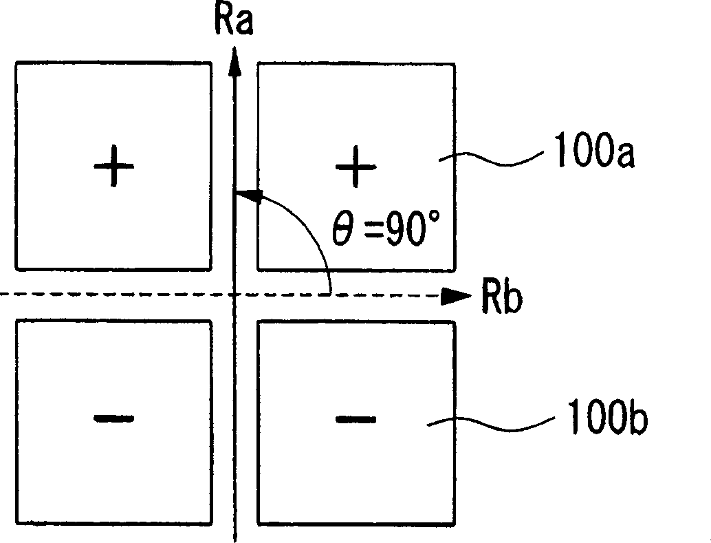
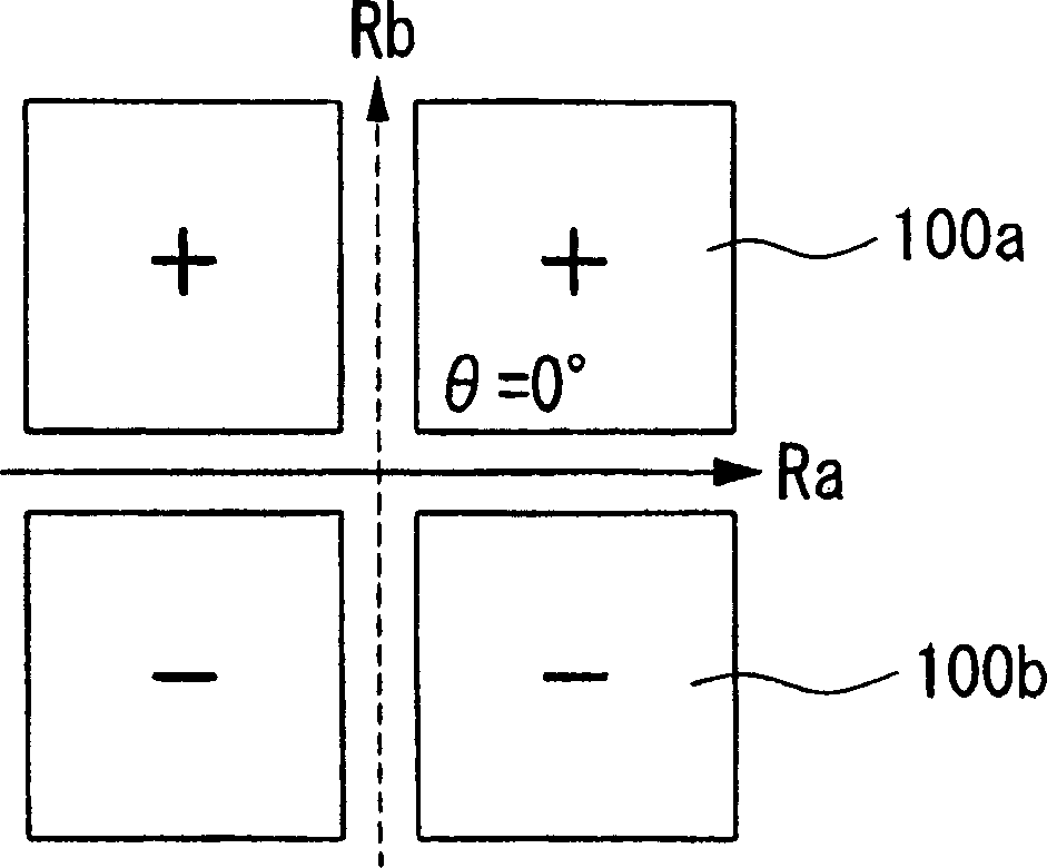
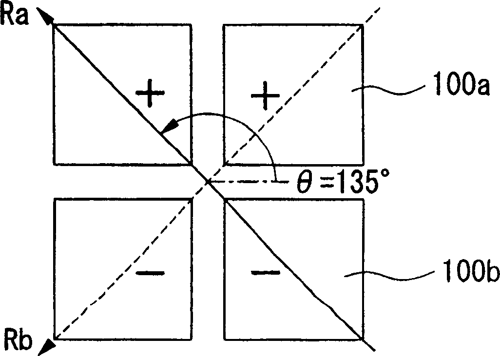
An active-matrix liquid crystal display is composed of an active matrix substrate, a liquid crystal, and an opposite substrate having a common electrode. The active matrix substrate fabricates a first group of pixel electrodes that are aligned and supplied with picture signals of a first polarit, and a second group of pixel electrodes that are aligned to adjoin with the first group of pixel electrodes respectively and are supplied witb picture signals of a second polari. An inorganic orientation film is formed on the surfac of the active matrix substrate to provide a first orientation direction (Ra) to its proximal liquid crystal moleclges, while an organic orientation film is formed on the surface ofthe opposite substrate to provide a second orientation direction Rb, rectangularly crossing the first oneenation direction, to its proximal liquid-crstal molecules.

Description

[0001] This application is a divisional application of application number 02108087.9. technical field [0002] The present invention relates to liquid crystal displays, in particular active matrix liquid crystal displays for use in electronic devices such as color image projectors, the displays having row inverse drive and column inverse drive operation. Background technique [0003] Typically, liquid crystal displays of the projection type (referred to as liquid crystal display projectors) employ active matrix liquid crystal displays as their liquid crystal light valves, which act as light modulators. An active-matrix liquid crystal display comprises an active-matrix substrate on which signal lines, electrodes and switching elements for pixels are constructed, and its opposite substrate with a common electrode, wherein the substrates are arranged opposite to each other. The sheets are separated from each other by a prescribed gap through the sealing material. Liquid crysta...

Claims


Application Information

Patent Timeline
Patent Type & Authority Applications(China)
IPC IPC(8): G02F1/136G02F1/1337G02F1/1343G02F1/139
CPCG02F2001/13373G02F2001/134381G02F1/134363G02F1/1396G02F1/13373G02F1/134381G02F1/136
Inventor 山崎泰志田中孝昭
Owner SEIKO EPSON CORP
Why Eureka
Try Eureka