Liquid crystal display substrate and liquid crystal display device
- Summary
- Abstract
- Description
- Claims
- Application Information
AI Technical Summary
Benefits of technology
Problems solved by technology
Method used
Image
Examples
first embodiment
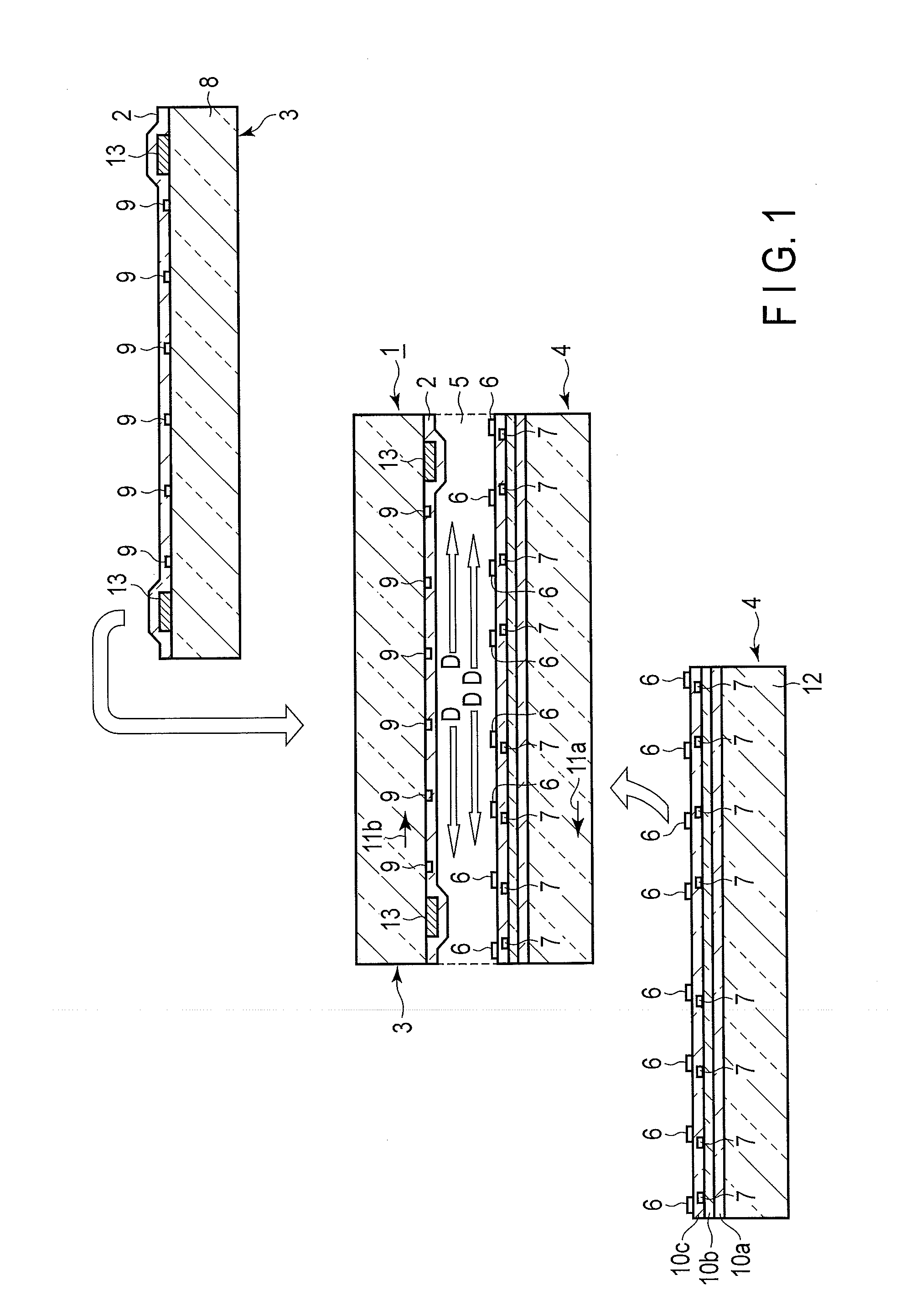
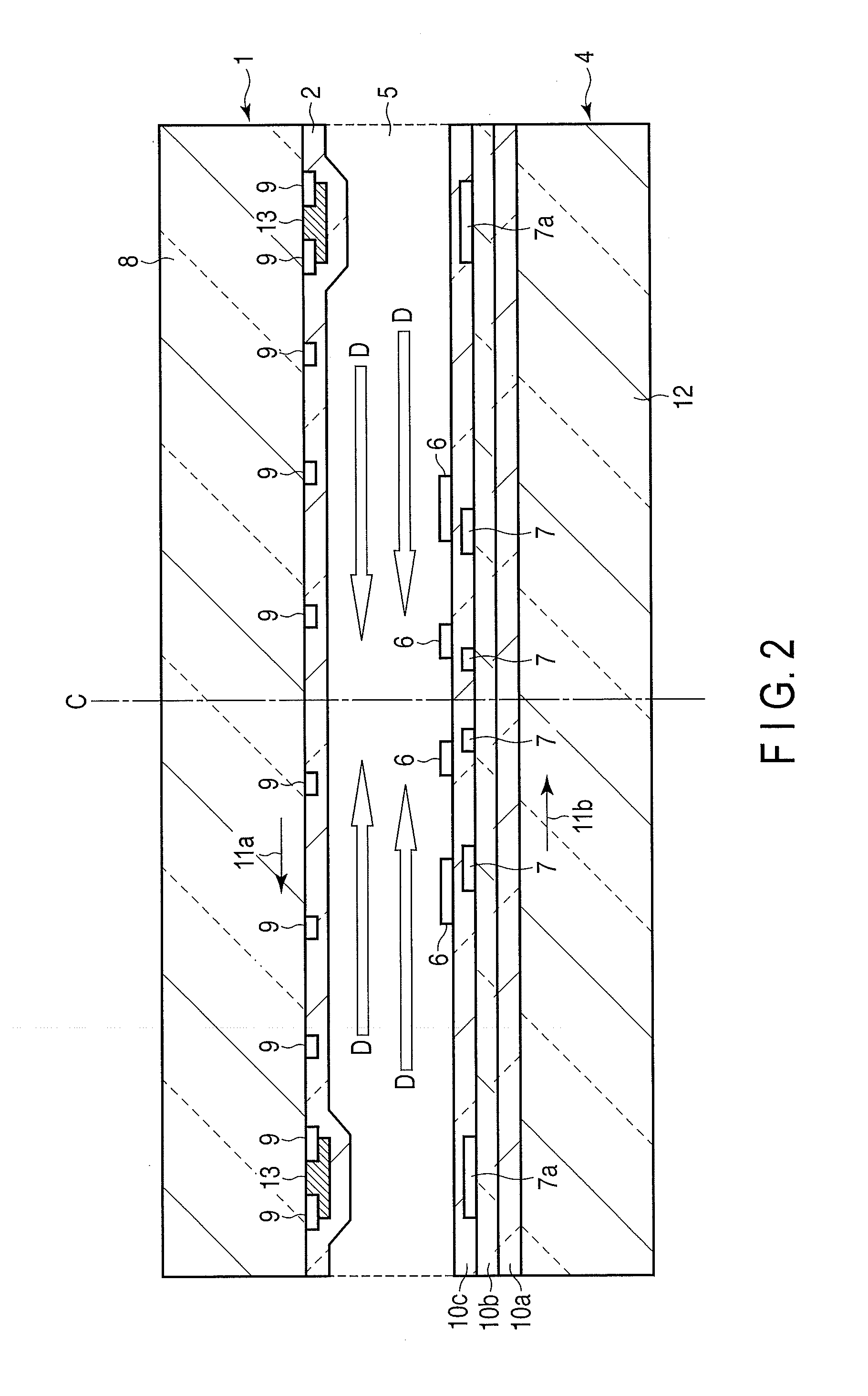
[0046]In the present embodiment, a liquid crystal display substrate which is adequate for liquid crystal driving based on an oblique electric field that is generated by a first electrode which is a pixel electrode of an array substrate equipped with an active element such as a thin film transistor (hereinafter, referred to as a TFT (Thin Film Transistor)), a second electrode of the array substrate, and a third electrode provided on a counter substrate; and a liquid crystal display device equipped with this liquid crystal display substrate, will be explained.
[0047]Meanwhile, a TFT may be formed by, for example, using a silicon semiconductor, or may be formed by using a complex metal-oxides semiconductor. When a TFT is formed by using the complex metal-oxides semiconductor, the aperture ratio of pixels or sub-pixels can be increased. Regarding a representative channel material for a TFT formed by using the complex metal-oxides semiconductor, for example, a complex metal-oxides of indi...
second embodiment
[0114]In the present embodiment, a counter substrate equipped with a color filter at the openings of a black matrix (color filter substrate) will be described.
[0115]FIG. 12 is a cross-sectional diagram illustrating an example of a liquid crystal display substrate according to the present embodiment.
[0116]In the liquid crystal display substrate 16 according to the present embodiment, a counter substrate 17 and the array substrate 4 face each other. The counter substrate 17 and the array substrate 4 are sealed together, with a liquid crystal layer 5 interposed therebetween.
[0117]To be more specific, the liquid crystal layer 5 is disposed above the top surface of the array substrate 4. The third electrode 9 is disposed above the top surface of the liquid crystal layer 5. Above the top surfaces of the liquid crystal layer 5 and the third electrode 9, the transparent resin layer 2 is disposed. Above the top surfaces of the transparent resin layer 2, a color filter 18 and the black matrix...
third embodiment
[0146]In the present embodiment, examples of the transparent resin, organic pigment and the like that can be used in the color filter 18 that has been described in the second embodiment will be explained.
[0147][Transparent Resin]
[0148]A photosensitive color composition used in the formation of a light shielding layer or a color layer contains a pigment dispersion, as well as a polyfunctional monomer, a photosensitive resin or a non-photosensitive resin, a polymerization initiator, a solvent and the like. Hereinafter, highly transparent organic resins that can be used in the present embodiment, such as photosensitive resins and non-photosensitive resins, are collectively referred to as transparent resins.
[0149]Transparent resins include thermoplastic resins, thermosetting resins, or photosensitive resins. Examples of the thermoplastic resins that may be used include a butyral resin, a styrene-maleic acid copolymer, chlorinated polyethylene, chlorinated polypropylene, polyvinyl chlori...
PUM
 Abstract
Description
Claims
Application Information


