Semiconductor device and method of manufacturing semiconductor device

a semiconductor device and semiconductor technology, applied in the field of semiconductor devices, can solve problems such as display failure in the display panel of the display device, and achieve the effect of improving the yield of the display device and reducing the display failure of the display devi

Active Publication Date: 2021-03-04
JAPAN DISPLAY INC
View PDF0 Cites 1 Cited by
  • Summary
  • Abstract
  • Description
  • Claims
  • Application Information

AI Technical Summary

Benefits of technology

[0007]An object of the present invention is to provide a technique that enables a reduction in the display failure of a display device and the improvement of the yields of the display device in a display device that adopts a semiconductor device including a thin film transistor using an oxide semiconductor.

Problems solved by technology

Therefore, in the display device that adopts a semiconductor device including a thin film transistor using an oxide semiconductor, a problem arises in that the properties of the TFT using an oxide semiconductor are shifted to the negative side and this shift causes display failure in the display panel of the display device.

Method used


Image

  • Semiconductor device and method of manufacturing semiconductor device
  • Semiconductor device and method of manufacturing semiconductor device
  • Semiconductor device and method of manufacturing semiconductor device

Examples


embodiment

Overall Structure Example of Display Device

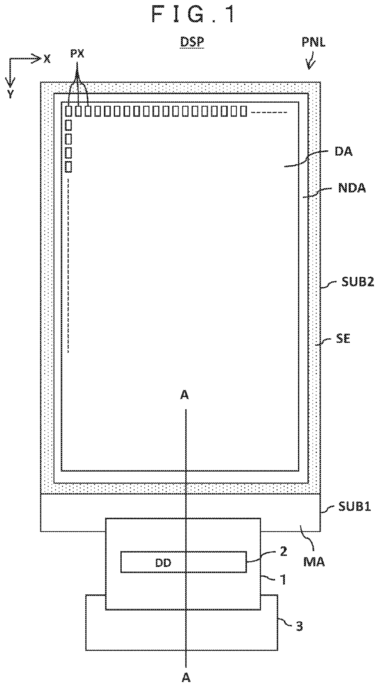
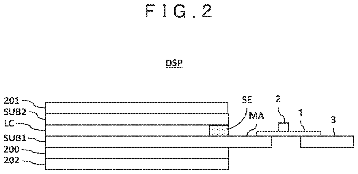
[0055]FIG. 1 is a plan view showing the appearance of a display device according to an embodiment. FIG. 2 is a cross sectional view taken along line A-A in FIG. 1. In FIGS. 1 and 2, a display device DSP includes a display panel PNL, a flexible printed circuit board 1, an IC chip 2, and a circuit board 3.

[0056]The display panel PNL is a liquid crystal display panel, and includes a first substrate (also referred to as a TFT substrate or an array substrate) SUB1, a second substrate (also referred to as a counter substrate) SUB2, a liquid crystal layer LC, and a sealing material SE.

[0057]The display panel PNL includes a display part (display region) DA that displays images and a non-display part (non-display region) NDA in a picture frame shape that surrounds the outer region of the display part DA. The second substrate SUB2 is opposite to the first substrate SUB1. The first substrate SUB1 has a mounting region MA extending in a second directio...


PUM

PropertyMeasurementUnit
temperatureaaaaaaaaaa
thicknessaaaaaaaaaa
thicknessaaaaaaaaaa

Abstract

There is provided a technique that enables a reduction in the display failure of a display device and the improvement of the yields of the display device in a display device that adopts a semiconductor device including a thin film transistor using an oxide semiconductor. A semiconductor device according to an embodiment includes a thin film transistor having an oxide semiconductor. The oxide semiconductor has a drain region, a source region, and a channel region provided between the drain region and the source region. The thin film transistor includes a gate insulating film provided on the channel region, an aluminum oxide film provided on the gate insulating film, an insulating film provided on the aluminum oxide film, and a gate electrode provided on the insulating film.

Description

CLAIM OF PRIORITY[0001]The present application claims priority from Japanese Patent Application JP 2019-153539 filed on Aug. 26, 2019, the content of which is hereby incorporated by reference into this application.BACKGROUND OF THE INVENTION[0002]The present invention relates to a semiconductor device, and more particularly to a semiconductor device, such as a display device having a thin film transistor using an oxide semiconductor.[0003]A liquid crystal display device is configured in which a TFT substrate is formed with pixels in a matrix configuration, the pixel has a pixel electrode, a thin film transistor (TFT), and other components, a counter substrate is disposed opposite to the TFT substrate, and a liquid crystal is sandwiched between the TFT substrate and the counter substrate. The optical transmittance of liquid crystal molecules is controlled at every pixel, and thus images are formed.[0004]Since a TFT using an oxide semiconductor has a small leakage current, this TFT is...

Claims


Application Information

Patent Timeline
Patent Type & Authority Applications(United States)
IPC IPC(8): H01L27/12H01L29/786H01L29/66
CPCH01L27/1225H01L29/66742H01L29/7869H01L27/1285H01L29/4908H01L27/1237H01L29/78633
Inventor WATAKABE, HAJIMEJINNAI, TOSHIHIDEONODERA, RYOHANADA, AKIHIRO
Owner JAPAN DISPLAY INC
Why Eureka
Try Eureka