Method for manufacturing light emitting device

A light-emitting device and manufacturing method technology, applied in semiconductor/solid-state device manufacturing, semiconductor devices, electrical components, etc., can solve problems such as reduced luminous efficiency, reduced surface cleanliness of lower electrodes, and changes in surface oxidation degree, so as to improve luminous efficiency , reduce the effect of display failure and reduce the degree of reduction

Inactive Publication Date: 2013-04-10
CANON KK
View PDF5 Cites 6 Cited by
  • Summary
  • Abstract
  • Description
  • Claims
  • Application Information

AI Technical Summary

Problems solved by technology

[0011] The first problem is that the reaction between the electrode material and the etching gas produces compounds on the surface of the lower electrode, and the re-attachment of the reaction products to the surface of the lower electrode reduces the cleanliness of the lower electrode surface
Decrease in cleanliness of the lower electrode surface leads to deterioration of hole or electron injection characteristics from the lower electrode into the organic layer
Therefore, a reduction in luminous efficiency, an increase in power consumption due to a higher driving voltage, or display failure such as uneven light emission occurs
In particular, when an alloy material containing Al or Ag is used for the lower electrode, a reactive compound with the etching gas is easily generated on the surface of the lower electrode, and such a problem is conspicuous
When a material such as indium tin oxide (ITO), indium zinc oxide (IZO) or magnesium oxide (MgO) is formed in the surface of the lower electrode x ) and the like, although no reactive compound is generated, the degree of surface oxidation of the oxide transparent conductive film changes, thereby deteriorating the hole or electron injection characteristics into the organic layer
[0012] The second problem is that due to the etching of the surface of the lower electrode, the surface smoothness is reduced to cause local concentration of current, thereby reducing the luminous efficiency
Therefore, the cleanliness or smoothness decreases the most on the surface of the lower electrode forming the organic EL layer of the third color
As a result, reduction in luminous efficiency or display failure frequently occurs in the organic EL element forming the organic EL layer of the third color, thereby reducing the yield of the organic EL display device

Method used


Image

  • Method for manufacturing light emitting device
  • Method for manufacturing light emitting device
  • Method for manufacturing light emitting device

Examples


Embodiment Construction

[0022] Various exemplary embodiments, features, and aspects of the invention will be described in detail below with reference to the accompanying drawings.

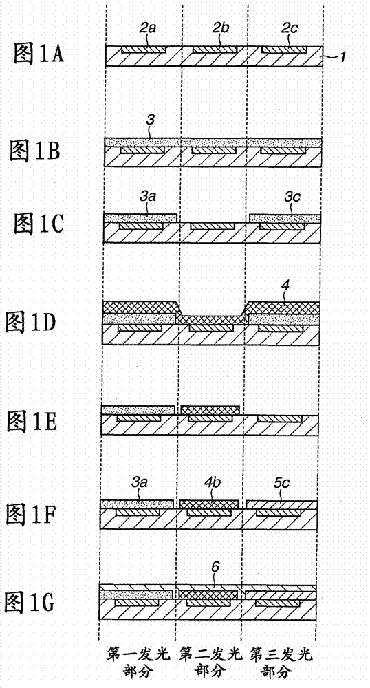
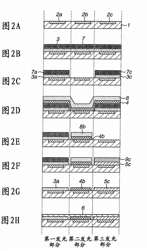
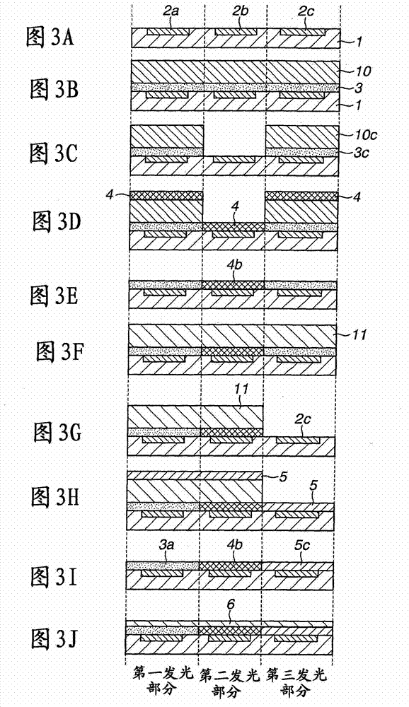
[0023] A light-emitting device manufactured by the method according to the present invention includes a light-emitting element typified by an organic electroluminescent element. The organic electroluminescent element includes a layer including an organic substance between a lower electrode and an upper electrode, and the organic substance includes an electroluminescent material of one of red, blue, or green. Three types of organic EL elements emitting light of these different colors are integrated as a group to constitute a pixel. In the case of an active matrix display device, a plurality of lower electrodes are individually formed on a substrate, and voltages are applied independently. The upper electrode is commonly used for all light emitting elements. In the case of a passive matrix, upper and lower electrodes are ...


PUM


Abstract

Provided is a method for manufacturing a light emitting device that includes, on a substrate, a plurality of lower electrodes, a first, a second and a third organic layers each formed on one of the lower electrodes to emit light of a color different from each other, and a upper electrode opposite to the lower electrodes sandwiching the first, the second or the third organic layer. The method includes forming the first organic layer on the plurality of lower electrodes, removing the first organic layer on a certain lower electrode to expose the lower electrode, and then forming a new organic layer on the exposed lower electrode, and repeating this processing for the second and third organic layers.

Description

technical field [0001] The present invention relates to a method of manufacturing a light emitting device. More specifically, the present invention relates to a method of manufacturing a light emitting device such as a display device or a lighting device including an organic electroluminescence (organic EL) element. Background technique [0002] In recent years, as a flat panel display, an organic EL display device, which is a self-luminous type device, has attracted attention. The organic EL display device means a display device using, as a display element, an organic EL element including a pair of electrodes and an organic layer disposed between the pair of electrodes. An organic EL display device that performs color display uses a configuration in which organic EL elements for emitting white light are combined with color filters of various colors, or for emitting light such as red, green, and blue. A plurality of types of organic EL elements of mutually different colors...

Claims


Application Information

Patent Timeline
Patent Type & Authority Applications(China)
IPC IPC(8): H01L51/56H01L27/32
CPCH10K59/35H10K71/00H10K71/231
Inventor 大重秀将
Owner CANON KK
Why Eureka
Try Eureka