Manufacturing method of multilayer printed circuit board

A multi-layer printing and circuit board technology, applied in the direction of printed circuit manufacturing, multi-layer circuit manufacturing, printed circuit, etc., can solve the problems of prolonging the manufacturing time, increasing the manufacturing cost, high impedance of the wall circuit layer, etc.

Inactive Publication Date: 2004-10-06
SAMSUNG ELECTRO MECHANICS CO LTD
View PDF0 Cites 16 Cited by
  • Summary
  • Abstract
  • Description
  • Claims
  • Application Information

AI Technical Summary

Problems solved by technology

[0036] That is, the conventional assembly process has a disadvantage in that, when the number of layers constituting the MLB is increased, the process of forming a via hole using a laser beam, the layer lamination process, and the plating process are repeated in sequence, prolonging the manufacturing time of the MLB, and when desired It is difficult to detect the MLB during the MLB manufacture, thereby undesirably increasing the defect ratio of the MLB, thus increasing the man

Method used


Image

  • Manufacturing method of multilayer printed circuit board
  • Manufacturing method of multilayer printed circuit board
  • Manufacturing method of multilayer printed circuit board

Examples


Embodiment Construction

[0052] Reference is now made to the drawings, wherein the same reference numerals are used in different drawings to designate the same or like parts.

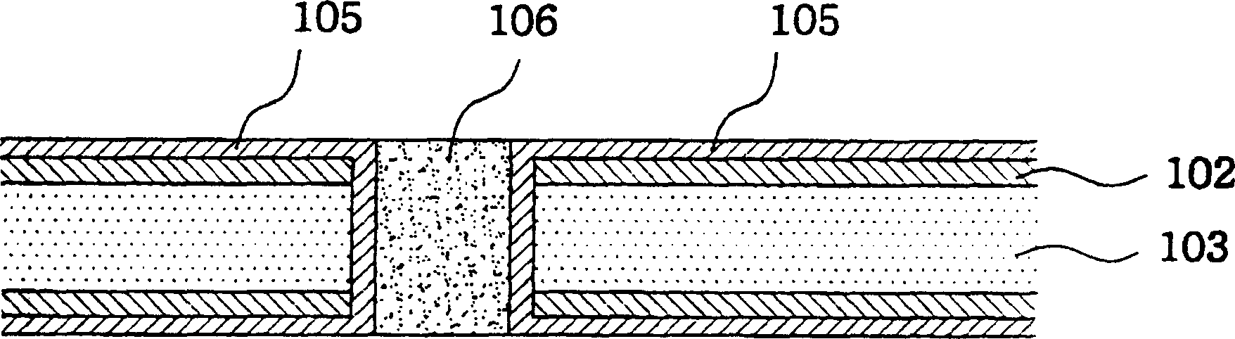
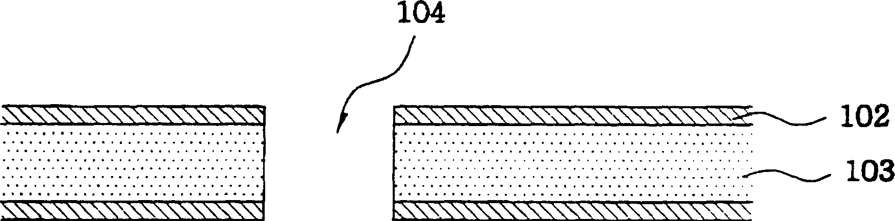
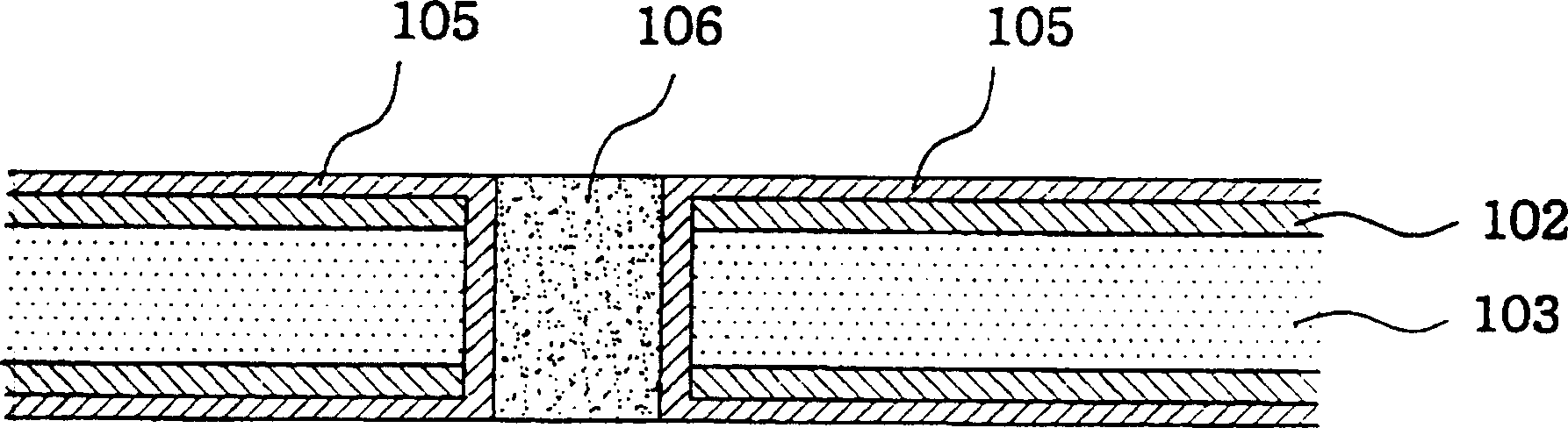
[0053] Figure 7 A lamination process of circuit layers and insulating layers is shown. The circuit layers 306a, 306b and 306c and the insulating layers 506a and 506b are respectively formed according to different processes, and they are arranged in a manner of alternately stacking the circuit layers and the insulating layers, such as Figure 7 shown, and then press them so that they touch each other in order to manufacture such as Figure 8 The six-layer PCB shown.

[0054] The different processes for making the circuit layer and insulating layer are now described.

[0055] 2A-2E are respectively cross-sectional views showing the fabrication of circuit layers constituting a multilayer PCB according to a first embodiment of the present invention, the fabrication process being performed according to a conventional technique. ...


PUM


Abstract

Disclosed is a method of fabricating a multi-layered PCB, wherein a plurality of circuit layers on which circuit patterns are constructed and insulating layers which are alternately positioned between the circuit layers to insulate the circuit layers from each other are severally fabricated according to different processes, and then layered with each other at once. The present invention provides a method of fabricating a multi-layered PCB, in which a copper clad laminate is drilled to create via holes therethrough in such a way that a diameter of each via hole is relatively small, and then plated with copper to plug the via holes with the copper, thereby omitting the plugging process of the via holes using paste. The insulating layers are formed in such a way that semi-hardened (b-stage) thermosetting resin layers are layered on both sides of a completely hardened (c-stage) thermosetting resin layer, thereby improving impedance balance of the insulating layer.

Description

technical field [0001] The present invention generally relates to methods of manufacturing multilayer printed circuit boards (MLBs). In particular, the present invention relates to a method of manufacturing a multilayer printed circuit board, wherein a plurality of circuit layers constituting a circuit pattern thereon and insulating layers alternately provided between the circuit layers to insulate the circuit layers from each other are respectively manufactured according to different processes , and then stack each other one at a time, which is different from the conventional assembly process. Background technique [0002] Those skilled in the art know that with the recent trend toward small, slim, highly integrated, small and portable electronic products, there is an increasing demand for finely patterned, small and small printed circuit boards (PCBs). In addition, the conventional substances used to form multilayer PCBs are replaced and the number of layers forming MLB i...

Claims


Application Information

Patent Timeline
IPC IPC(8): H05K3/40H05K3/42H05K3/46
CPCH05K2203/1461H05K3/462H05K2201/10378H05K2201/0959H05K2201/09536H05K2201/0355H05K2203/0554H05K2201/0195H05K3/4069H05K2201/096H05K3/427Y10T29/49165Y10T29/49128Y10T29/49156H05K3/46
Inventor 金應秀康丈珪睦智秀李存台宋昌奎宣炳国
Owner SAMSUNG ELECTRO MECHANICS CO LTD
Why Eureka
Try Eureka