Optical waveguide ,light source device ,display device and information terminal configured with them

A technology of a display device and a light source device, which is applied in the directions of light guide, light source, electric light source, etc., can solve the problems that light cannot be reflected, the recognition rate of the display device becomes low, and the optical utilization efficiency of the light source device decreases, and achieves high emission efficiency and intensity distribution. uniform effect

Active Publication Date: 2004-12-01
HANNSTAR DISPLAY CORPORATION
View PDF4 Cites 9 Cited by
  • Summary
  • Abstract
  • Description
  • Claims
  • Application Information

AI Technical Summary

Problems solved by technology

[0033] However, in the case of this structure, since the depth of the grooves is limited by the pitch of the grooves and the angle of the grooves, among the light incident on the optical waveguide, almost parallel light cannot be effectively reflected on the grooves.
As a result, optical loss becomes large due to repeated reflection of light within the optical waveguide or light is emitted from an incident surface opposite to that on which it was incident, resulting in a decrease in the optical utilization efficiency of the light source device.
That is to say, the light emitted from the optical waveguide is uniform when the utilization efficiency is low, and the resolution of the display device using this optical waveguide also becomes low.

Method used


Image

  • Optical waveguide ,light source device ,display device and information terminal configured with them
  • Optical waveguide ,light source device ,display device and information terminal configured with them
  • Optical waveguide ,light source device ,display device and information terminal configured with them

Examples


no. 1 example

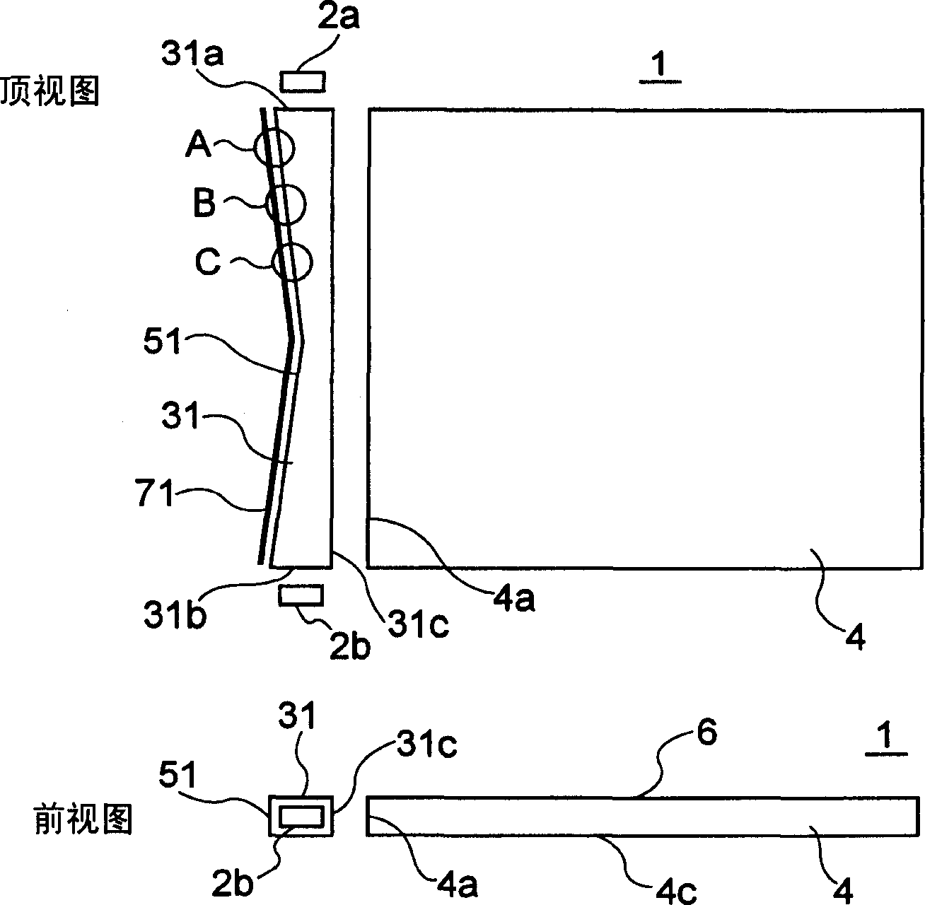
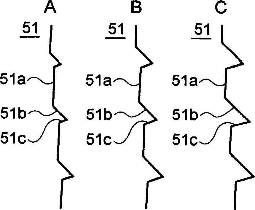
[0081] A first embodiment of the present invention will be described below. FIG. 1 shows the structure of a light source device according to the present invention. Figure 1A is a brief top view and front view of the light source device 1, Figure 1B yes Figure 1A An enlarged view of the reflective portion 51 in portions A, B, and C of the linear optical waveguide 3 shown, and Figure 1C An enlarged view of the reflective portion 6 in the sheet-shaped optical waveguide 4 . Figure 1D A diagram showing the relationship between each part of the reflector 51 is shown.

[0082] The light source device 1 has point light sources 2 ( 2 a and 2B ), a linear optical waveguide 31 , a sheet-shaped optical waveguide 4 , and a reflection surface 71 .

[0083] Each point light source 2a and 2b is a light source sufficiently small in the light emission area of ​​the light source device 1, for example, a light emitting diode LED may be used but not limited thereto, a small light source s...

no. 2 example

[0108] A second preferred embodiment of the present invention will be described below. Fig. 3 shows a light source arrangement 1 according to the invention. Figure 3A is a brief top view and front view of the light source device 1, Figure 3B yes Figure 3A An enlarged view of the reflective portion 52 in portions A, B, and C of the linear optical waveguide 32 shown, and Figure 3C It is an enlarged view of the reflective portion 6 of the sheet-shaped optical waveguide 4 .

[0109] Similar to the first embodiment, the light source device 1 has point light sources 2 ( 2 a and 2 b ), linear optical waveguides 32 , sheet-shaped optical waveguides 4 , and reflective surfaces 72 .

[0110]The point light sources 2 (2a and 2b), the sheet-shaped optical waveguide 4, and the reflective surface 72 are the same as those of the first embodiment. Although the linear optical waveguide 32 is almost the same as the linear optical waveguide 31 of the first embodiment, the reflective part...

no. 3 example

[0117] A third preferred embodiment of the present invention will be described below. FIG. 5 shows the light source device 1 according to the present embodiment. Figure 5A is a brief top view and front view of the light source device 1, Figure 5B show Figure 5A An enlarged view of the reflective portion 63 in the A, B, and C portions of the sheet-shaped optical waveguide 43 shown.

[0118] The light source device 1 has a sheet-shaped optical waveguide 43, a reflection surface 73, line light sources 8 (8a and 8b), and reflectors 9 (9a and 9b).

[0119] Such as Figure 5A As shown in , the reflective surface 73 is provided close to the reflective portion 63 of the sheet-shaped optical waveguide 43 . In addition, the reflectors 9 a and 9 b have approximately the same thickness as the sheet-shaped optical waveguide, and improve the incident efficiency of light emitted from the line light sources 8 a and 8 b to the sheet-shaped optical waveguide 43 .

[0120] The line light...


PUM


Abstract

A light source device which is uniform in the intensity of distribution of an emitted light and high in the optical utilization efficiency, a display device which is high in recognability and is energy-saving, and an information terminal are provided. A reflecting portion is formed on a surface opposed to an emitting surface of a linear light guide. The reflecting portion is periodically formed with a total reflecting surface guiding a light incident on a linear light guide from a point light source, a light extracting surface allowing the light to reflect in such a way as to emit the light guiding the linear light guide from the emitting surface, and a re-incidence plane which takes the light transmitted but not reflected on the light extracting surface into the linear light guide again. By changing the size of the light extracting surface and the re-incidence plane, the intensity of distribution of the emitting light from the linear light guide can be made uniform.

Description

technical field [0001] The present invention relates to an optical waveguide, a light source device equipped with an optical waveguide, a display device and an information terminal using the light source device, and particularly relates to a light source device having an optical waveguide with uniform intensity distribution of emitted light and high emission efficiency, and a high recognition rate and Display devices requiring less power consumption, and information terminals equipped with them. Background technique [0002] Among display devices, a liquid crystal display (LCD) is characterized by light weight and thin volume. Accordingly, LCDs have been widely used as display devices for portable, notebook-type information processing terminals and the like, or as display devices for information terminals including, for example, portable televisions, electronic notebooks, portable phones, and the like. Generally in an LCD, the visibility of information is enhanced by illumi...

Claims


Application Information

Patent Timeline
Patent Type & Authority Applications(China)
IPC IPC(8): G02B6/00F21S2/00F21V8/00F21Y101/02G02F1/13357
CPCG02B6/0046G02B6/0038G02B6/0028G02B6/0061
Inventor 八木淑惠今井雅雄斋藤悟郎三村广二
Owner HANNSTAR DISPLAY CORPORATION
Why Eureka
Try Eureka