Probe connecting structure for detecting tool of printed circuit board
A printed circuit board and connection structure technology, applied in the field of printed circuit board inspection tools, can solve the problems of poor conduction, high manufacturing cost, increased wiring density, etc., and achieve the effects of convenient production, simple structure, and avoidance of bending under pressure
- Summary
- Abstract
- Description
- Claims
- Application Information
AI Technical Summary
Problems solved by technology
Method used
Image
Examples
Embodiment 1
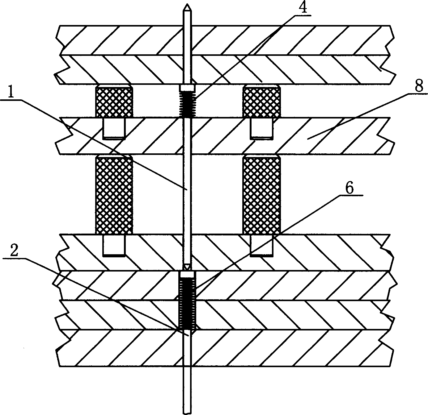
[0019] Embodiment one: see attached figure 1 to attach Figure 4 As shown, a probe connection structure for a printed circuit board inspection tool includes a probe 1 and a probe contact terminal 2. The probe 1 is an elongated needle-shaped structure with a tapered lower end surface. About one-third of the upper part of the needle 1 is provided with a boss 3 that cooperates with the return spring 4. The boss 3 is a cylindrical protrusion with an integral structure with the probe 1, and the contact terminal 2 of the probe is connected to the wire 7. , its upper end forms a thicker head 5, which is formed by punching the adjacent ends of the covered wires, and forms a concave structure on the upper end surface that matches the lower end of the probe 1. For example, it can be disclosed in the Chinese invention patent application CN1445551A The lower end of probe 1 is in contact with the upper end of probe contact terminal 2.
[0020] When in use, it is installed on the plate 8 ...
PUM
 Abstract
Description
Claims
Application Information


