CIS image acquisition method for bore diameter and bore number detection of printed circuit board

A printed circuit and image acquisition technology, applied in the field of image processing and computer vision, can solve the problems of complex image acquisition and manufacturing process of hole inspection machine, strict image registration requirements, and strict position requirements, and achieves the reduction of equipment cost and production process. Low complexity, low requirements for image registration, and reduced equipment cost

Inactive Publication Date: 2005-01-26
BEIJING INSTITUTE OF TECHNOLOGYGY
View PDF0 Cites 3 Cited by
  • Summary
  • Abstract
  • Description
  • Claims
  • Application Information

AI Technical Summary

Problems solved by technology

[0003] 1. Expensive: Due to the cost and process requirements of the CCD sensor itself, the price of PCB inspection equipment using CCD sensors on the market is as high as 600,000 yuan or more. This high-priced product makes many PCB manufacturers reduce the inspection equipment as much as possible. Purchase quantity
[0004] 2. The manufacturing process of the image acquisition part of the hole inspection machine is complicated: due to the small field of view of the CCD sensor lens system, the width of the printed circuit board produced is much larger than the width that the lens can cover
Therefore, most of the existing products use dense multi-number CCDs or mobile CCDs for image acquisition, which makes the manufacturing process of the image acquisition part complicated and requires high precision. The general assembly accuracy is required to be around 0.001mm
[0005] 3. Strict requirements for image registration: Some hole inspection machines have strict requirements on the placement of printed circuit boards, and there are even devices that require fixed placement

Method used


Image

  • CIS image acquisition method for bore diameter and bore number detection of printed circuit board
  • CIS image acquisition method for bore diameter and bore number detection of printed circuit board
  • CIS image acquisition method for bore diameter and bore number detection of printed circuit board

Examples


Embodiment Construction

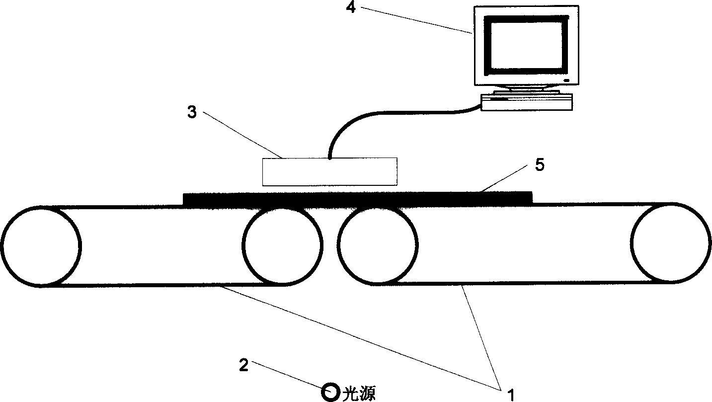
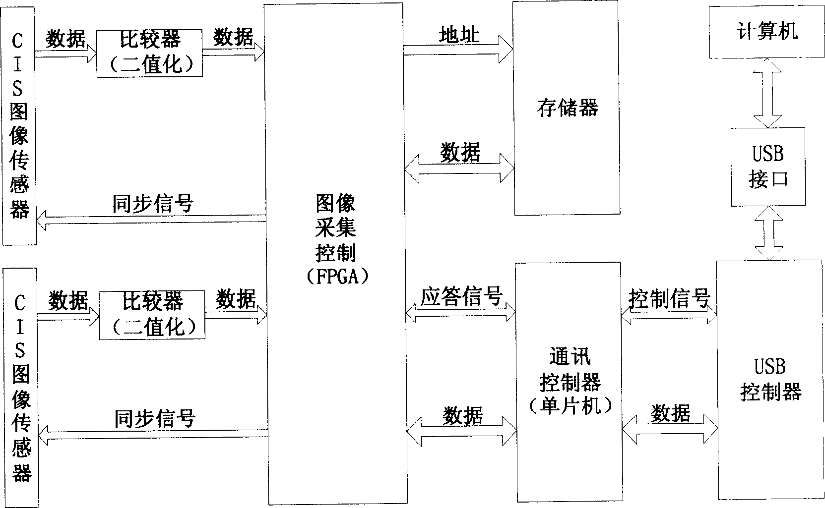
[0027] exist figure 1 Among them, the printed circuit board (5) to be detected is placed on the printed circuit board conveying device (1), and is driven by the motor to move along the surface of the conveying belt at a constant speed. The transmitted light source (2) is placed on two adjacent PCB conveying devices. Just below the slit between the rollers, the PCB printed circuit board is irradiated upward through the slit, and the light irradiated to the through hole on the circuit board can be received by the CIS image sensor of the image acquisition part (3) through the circuit board, and the formed The image is bright, but the place where there is no via hole on the circuit board is dark on the CIS image sensor because there is no light passing through. The brightness information obtained by the CIS image sensor is binarized, compressed and stored in the image acquisition The memory of part (3) is transmitted to the memory of computer (4) by the communication module of ima...


PUM


Abstract

It is a method to access CIS image from real-time on-line printing board verifier. This method substitutes CIS image sensor for OCD image sensor to be used as components of image access and to constitute the printing board verifier. This method is featured with low cost and simple process by employing such printing board verifier.

Description

Technical field [0001] The invention belongs to the technical fields of image processing and computer vision. Background technique [0002] Image processing and computer vision are widely used in the manufacturing industry, especially in product inspection, process monitoring, measurement and assembly tasks. In the production process of printed circuit board (referred to as: PCB), it is a key link to inspect and control product quality. In order to solve the problem of unstable detection quality in manual detection, people have developed a variety of dedicated online quality detection systems. In the current PCB hole inspection machine market, the devices that can be seen generally use different numbers of CCD image sensors, and use non-contact detection methods such as transmitted light to obtain images. For example, the HC-610 produced by Taiwan Yaya Technology adopts CCD image sensor and transmitted light detection method, adopts high-frequency light source, and its ape...

Claims


Application Information

Patent Timeline
Patent Type & Authority Applications(China)
IPC IPC(8): G01B21/14
Inventor 刘万春朱玉文潘云东裴明恩刘俐
Owner BEIJING INSTITUTE OF TECHNOLOGYGY
Why Eureka
Try Eureka