
Organic luminous display element and its producing method

A technology of light-emitting display and organic light-emitting layer, which is applied in electrical components, light-emitting materials, electroluminescent light sources, etc., and can solve the problems of rising driving voltage of components, reducing efficiency, and affecting the life of components.

Active Publication Date: 2005-03-02
AU OPTRONICS CORP
View PDF0 Cites 11 Cited by
  • Summary
  • Abstract
  • Description
  • Claims
  • Application Information

AI Technical Summary

Problems solved by technology

However, increasing the thickness of the hole transport layer will increase the driving voltage of the device, reduce the efficiency, and affect the life of the device

Method used


Image

  • Organic luminous display element and its producing method
  • Organic luminous display element and its producing method
  • Organic luminous display element and its producing method

Examples


Embodiment Construction

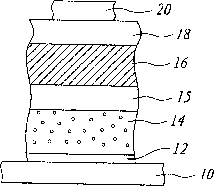
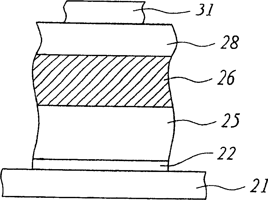
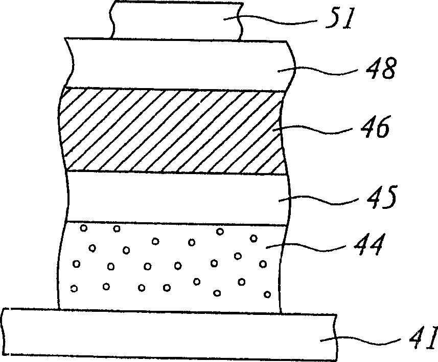
[0036] The structure of two groups of control groups and the structure of an embodiment of the present invention are proposed below, and related experimental processes and results are proposed. The relationship between the relative luminescence (Relative Luminescence) and the operation time (Operational Time) of the three groups of component structures is as follows: image 3 shown. The relationship between the driving voltage (Voltages) and the operating time (Operational Time) of the three-group element structure is as follows: Figure 4 shown.

[0037] first control group

[0038] Figure 2A It is a schematic structural diagram of the organic light-emitting display element of the first control group of the present invention. First, ITO is provided and subjected to UV ozone treatment to form the anode 21 . A carbon fluoride (CFx) film is then formed on the anode 10 by plasma deposition to serve as the hole injection layer 22 . Then NPB is evaporated on the hole injec...


PUM


Abstract

An organic luminous display unit includes an anode, a hole injection layer formed on the anode, a first hole transmission layer formed on the injection layer and the said transmission layer is doped by p type dopants, a second hole transmission layer formed on the first layer, an organic luminous layer formed on the second hold transmission layer, an electronic transmission layer formed on the organic luminous layer and a cathode formed on the electronic transmission layer, among which, the injection layer is matched with the first transmission layer for increasing the element stability and life.

Description

technical field [0001] The present invention relates to an organic light emitting display element and a manufacturing method thereof, and in particular to an organic light emitting display element with long service life and high stability and a manufacturing method thereof. Background technique [0002] Organic Electroluminescence Device (Organic Electroluminescence Device), also known as Organic Light Emitting Diode (OLED), due to its simple structure, excellent operating temperature and response speed, sharp color contrast, and no viewing angle restrictions, etc. Advantages, has been widely used in flat-panel displays. [0003] The organic light-emitting display device has a multi-layer structure, mainly an organic light-emitting layer is formed between the cathode and the anode to generate electroluminescence. Between the organic light emitting layer and the anode, a hole injection layer and a hole transport layer are formed, and between the organic light emitting layer ...

Claims


Application Information

Patent Timeline
IPC IPC(8): C09K11/06H05B33/10H05B33/12H05B33/20H05B33/26
Inventor 游宗烨
Owner AU OPTRONICS CORP
Learn More