Organic light-emitting device and manufacturing method thereof

An electroluminescence device and luminescence technology, applied in the direction of electric solid-state devices, chemical instruments and methods, semiconductor/solid-state device manufacturing, etc., can solve the problems of film layer damage, regeneration ability attenuation, cost increase, etc. The ability to inject, reduce the process steps, and facilitate the effect of injection and transmission

Inactive Publication Date: 2013-10-30
OCEANS KING LIGHTING SCI&TECH CO LTD +1
View PDF4 Cites 1 Cited by
  • Summary
  • Abstract
  • Description
  • Claims
  • Application Information

AI Technical Summary

Problems solved by technology

At present, most of the research is to use two or more materials with hole injection or electron injection as the charge generation layer (such as Cs:BCP / V 2 o 5 ), or n-type and p-type doped layers as charge generation layers (such as n-type (Alq 3 :Li) and p-type (NPB:FeCl 3 )), or Al-WO 3 -Au, etc. are sequentially connected to multiple light-emitting units, but this charge generation layer will have reactions between different metal compounds, resulting in varying degrees of attenuation of regeneration ability or damage to the film layer. At the same time, this type of doped There are many types of materials required for miscellaneous, and the cost will also rise accordingly.

Method used


Image

  • Organic light-emitting device and manufacturing method thereof
  • Organic light-emitting device and manufacturing method thereof

Examples


preparation example Construction

[0047] The preparation method of the above-mentioned laminated organic electroluminescent device comprises the following steps:

[0048] S1. First conduct photolithographic treatment on the conductive anode substrate, and then use detergent, deionized water, acetone, ethanol, and isopropanol to ultrasonically clean each for 15 minutes to remove organic pollutants on the glass surface

[0049] S2. After cleaning, perform oxygen plasma treatment on the conductive anode substrate for 5-15 minutes, and the power is 10-50W;

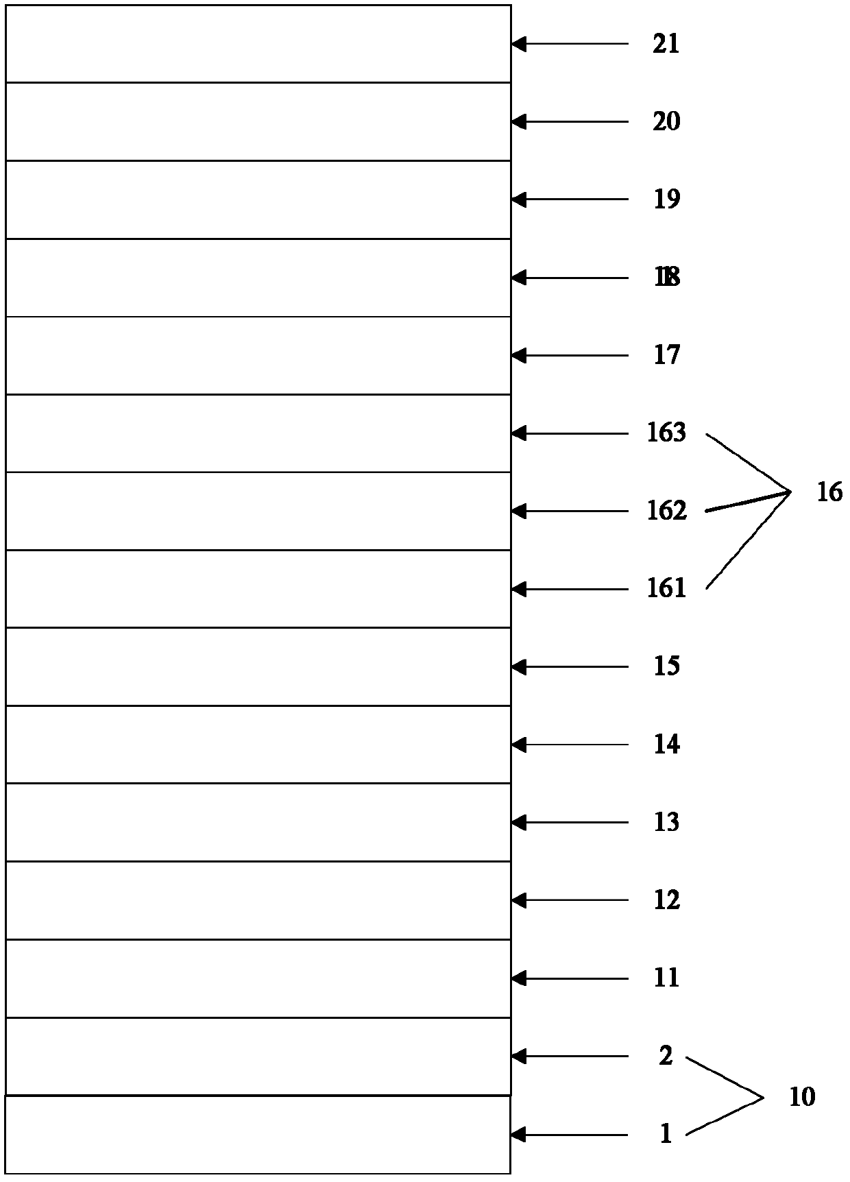
[0050] S3. Using an evaporation process, the surface of the conductive anode substrate treated with oxygen plasma in step S2 is sequentially laminated with an evaporated hole injection layer, a first hole transport layer, a first light emitting layer, a first electron transport layer and a first electron injection layer. layer;

[0051] S4, then, prepare a charge regeneration layer on the surface of the first electron injection layer, the charge regeneration ...

Embodiment 1

[0062] The organic electroluminescent device structure of this embodiment: glass / ITO / MoO 3 / NPB / Alq 3 / TAZ / CsF / (TAZ:MoO 3 / MoO 3 / TCTA:MoO 3 ) / NPB / Alq 3 / TAZ / CsF / Al.

[0063] The preparation process of the organic electroluminescent device is as follows:

[0064] First, photolithographically process the ITO glass substrate, cut it into the required size, and then use detergent, deionized water, acetone, ethanol, and isopropanol to sonicate for 15 minutes each to remove organic pollutants on the glass surface;

[0065] After cleaning, conduct proper treatment on the conductive substrate: treat the conductive anode layer (ITO) with oxygen plasma, the treatment time is 5min, and the power is 30W;

[0066] On the surface of the ITO layer, the vapor-deposited hole injection layer (the material is MoO 3 , thickness is 40nm), the first hole transport layer (material is NPB, thickness is 40nm), the first light-emitting layer (material is Alq 3 , thickness is 30nm), the first e...

Embodiment 2

[0071] The organic electroluminescent device structure of this embodiment: glass / IZO / WO 3 / TCTA / BCzVBi / Bphen / Cs 2 CO 3 / (TPBi:MoO 3 / MoO 3 / NPB:MoO 3 ) / NPB / DCM / Bphen / CsN 3 / Ag.

[0072] The preparation process of the organic electroluminescent device is as follows:

[0073] First, photolithographically process the IZO glass substrate, cut it into the required size, and then use detergent, deionized water, acetone, ethanol, and isopropanol to sonicate for 15 minutes each to remove organic pollutants on the glass surface;

[0074] After cleaning, conduct appropriate treatment on the conductive substrate: oxygen plasma treatment of the conductive anode layer (IZO), the treatment time is 5min, and the power is 30W;

[0075] On the surface of the IZO layer, the vapor-deposited hole injection layer (the material is WO 3 , thickness is 20nm), the first hole transport layer (the material is TCTA, the thickness is 60nm), the first light-emitting layer (the material is BCzVBi, t...


PUM

PropertyMeasurementUnit
Thicknessaaaaaaaaaa
Thicknessaaaaaaaaaa
Thicknessaaaaaaaaaa

Abstract

The invention belongs to the field of organic light-emitting devices and discloses an organic light-emitting device and a manufacturing method thereof. The organic light-emitting device comprises a conductive anode substrate, a hole injection layer, a first hole transmission layer, a first luminous layer, a first electron transmission layer, a first electron injection layer, a charge regeneration layer, a second hole transmission layer, a second luminous layer, a second electron transmission layer, a second electron injection layer and a cathode layer, wherein the conductive anode substrate, the hole injection layer, the first hole transmission layer, the first luminous layer, the first electron transmission layer, the first electron injection layer, the charge regeneration layer, the second hole transmission layer, the second luminous layer, the second electron transmission layer, the second electron injection layer and the cathode layer are sequentially stacked, and the charge regeneration layer comprises an n-type layer, a middle layer and a p-type layer. According to the organic light-emitting device, the p-type layer of the charge regeneration layer provides holes, the n-type layer of the charge regeneration layer provides electrons, metal oxide of the middle layer can improve electron and hole regeneration capacity and electrical conductivity of the charge regeneration layer, all the n-type layer, the middle layer and the p-type layer comprise the same metal oxide, the potential barrier between the layers can be reduced, injection and transmission of holes or electrons are facilitated, and the luminous efficiency of the organic light-emitting device is improved.

Description

technical field [0001] The invention relates to the field of electroluminescent devices, in particular to an organic electroluminescent device and a preparation method thereof. Background technique [0002] In 1987, C.W.Tang and Van Slyke of Eastman Kodak Company in the United States reported a breakthrough in the research of organic electroluminescence. A high-brightness, high-efficiency double-layer organic electroluminescent device (OLED) was prepared by using ultra-thin film technology. In this double-layer structure device, the brightness reaches 1000cd / m at 10V 2 , its luminous efficiency is 1.51lm / W, and its lifespan is more than 100 hours. [0003] The principle of OLED light emission is based on the action of an external electric field, electrons are injected from the cathode to the lowest unoccupied molecular orbital (LUMO) of organic matter, and holes are injected from the anode to the highest occupied orbital (HOMO) of organic matter. Electrons and holes meet,...

Claims


Application Information

Patent Timeline
IPC IPC(8): H01L51/52H01L51/54H01L51/56C09K11/06
Inventor 周明杰王平黄辉陈吉星
Owner OCEANS KING LIGHTING SCI&TECH CO LTD
Why Eureka
Try Eureka