Supercharge Your Innovation With Domain-Expert AI Agents!

Method for manufacturing stamper, stamper and optical recording medium

A stamper and plasma technology, which is used in the field of manufacturing stampers, stampers and optical recording media, can solve the problems of reduced electrical conductivity, environmental problems, and reduced formation rate of electroformed thin films.

Inactive Publication Date: 2005-03-09
PANASONIC CORP
View PDF2 Cites 2 Cited by
  • Summary
  • Abstract
  • Description
  • Claims
  • Application Information

AI Technical Summary

Problems solved by technology

[0011] (1) Because the electrical conductivity of nickel thin film reduces, so the film formation rate of electroforming thin film (II) 207 will reduce;
[0012] (2) If the surface of the nickel thin film is not uniformly formed after the oxidation process, the thickness of the resulting stamper will vary since the film formation rate of the electroformed thin film (II) 207 will vary over the entire surface;
[0014] (4) The liquid waste from the oxidation process in question (1) will cause environmental problems

Method used


Image

  • Method for manufacturing stamper, stamper and optical recording medium
  • Method for manufacturing stamper, stamper and optical recording medium

Examples


example 1

[0050] (1)

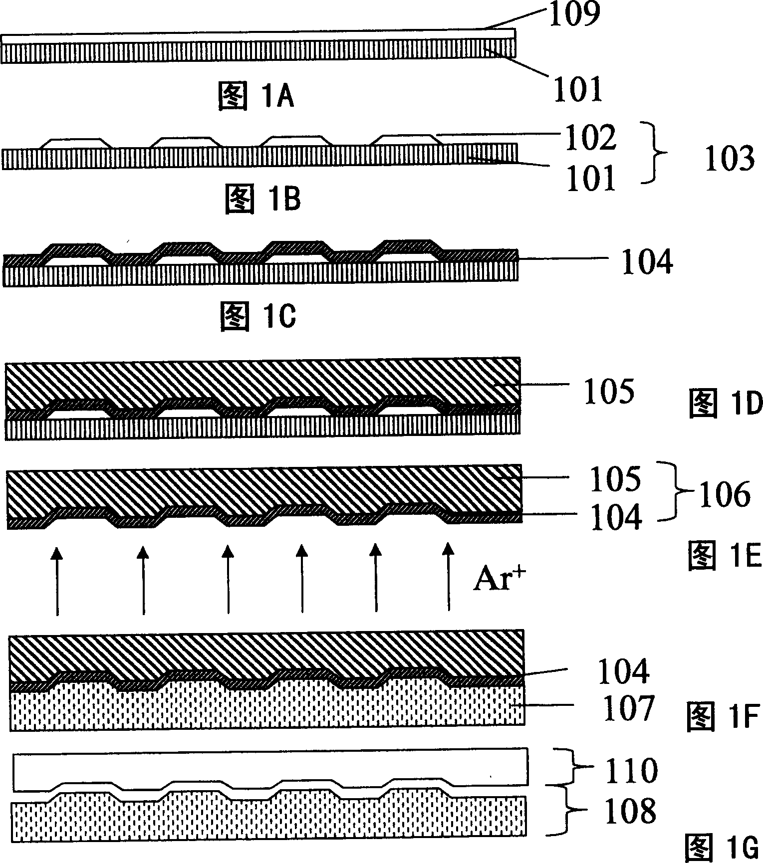
[0051] Examination of the dependence of the input power with respect to the etching process The experiments used to determine the etching conditions are described. Note that since the time dependence during etching is not critical, it is assumed to be constant at 90 s.

[0052] The results are shown in Table 1.

[0053] [Table 1]

[0054] Etched Input Power (W) Separability Noise (dBm)

[0055] 10 Poor N / A

[0056] 30 Poor N / A

[0057] 50 good -71

[0058] 200 good -73

[0059] 500 good -72

[0060] 600 good -68

[0061] 800 good -65

[0062] 1000 good -58

[0063] In Table 1, the term "poor" in the column of separability indicates an etching condition under which the electroformed film (II) 107 cannot be separated from the parent stamper 106, or indicates that defects are generated on the electroformed film (II) 107 conditions of. The term "good" in the same column indicates the condition that the mother stamper 108 without defe...

example 2

[0078] (1)

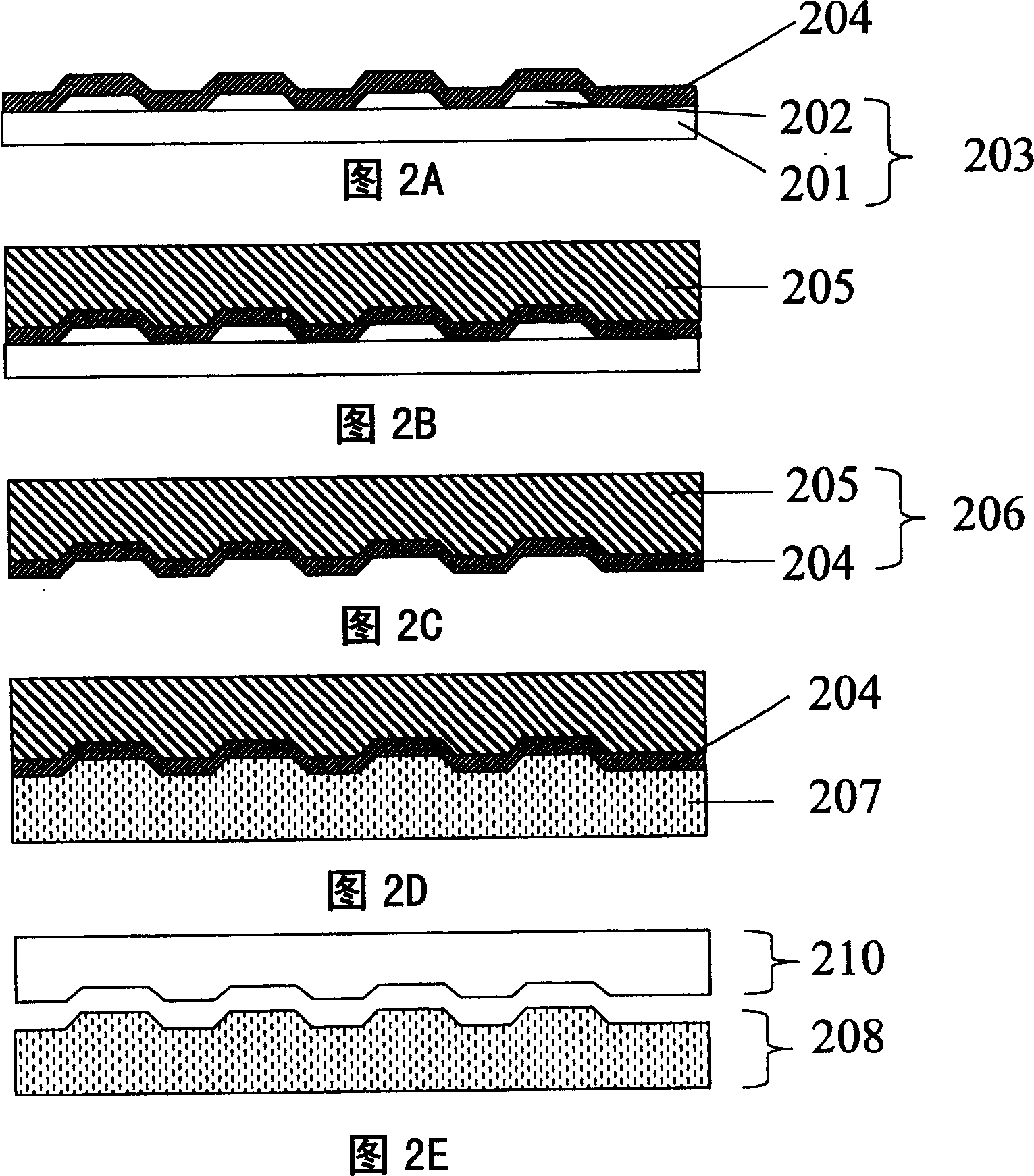
[0079] In Example 2, the master mold 108 will be formed through the same steps and processes as described above. Figure 1 will be used to describe this.

[0080] It is conceivable that there is a relationship between the separability of the mother stamper 108 , the presence of defects on the stamper, and whether nickel hydroxide can be uniformly formed on the parent stamper 106 . In order to form hydroxide uniformly on the stamper, it is necessary to immerse the stamper in water immediately after the plasma surface treatment. Conversely, after processing, if the parent stamper 106 is left in the atmosphere, nickel oxide and nickel hydroxide are produced. Since the ratio of nickel oxide to nickel hydroxide is locally different, and the separability of these materials is different, the difference in separability may locally occur, and the possibility that defects remain on the mother stamper 108 increases.

[0081] In Table 3, the relationship between the time th...


PUM

PropertyMeasurementUnit
thicknessaaaaaaaaaa
thicknessaaaaaaaaaa

Abstract

When producing a second stamper by forming a nickel electroformed film on a father stamper having patterns of pits and lands, defects appear on the second stamper during the stage of separating the second stamper from the father stamper. The object of the present invention is to decrease these defects. A method for manufacturing a stamper comprises performing a plasma surface treatment on a surface of a father stamper 106 having patterns of pits and lands, forming a nickel electroformed film (II) 107 on the surface of the father stamper 106, and separating the nickel electroformed film (II) 107 from the father stamper 106 so as to form a mother stamper 108.

Description

technical field [0001] The present invention relates to a method for manufacturing a stamper of a disc-shaped optical disc for reproducing information, a stamper, and an optical recording medium. Background technique [0002] Optical recording media for recording and reproducing information based on the application of light beams are widely used, and it is expected that the recording density will increase in the future. [0003] Recently, various optical discs capable of reproducing many images, a large amount of voice data, and digital data have been developed. Research directions are also directed towards the manufacture of discs with higher recording densities. [0004] Conventional stampers for forming optical recording media for recording and reproducing information by optical means such as lasers are known. Optical recording medium tracking grooves, and pits and land patterns corresponding to information pits are formed on the optical recording medium stamper. The o...

Claims


Application Information

Patent Timeline
Patent Type & Authority Applications(China)
IPC IPC(8): B29D17/00C25D1/00C25D1/22G11B7/24G11B7/26
CPCG11B7/263C25D1/22B29D17/005G11B7/26
Inventor 川口优子富山盛央
Owner PANASONIC CORP
Features
  • R&D
  • Intellectual Property
  • Life Sciences
  • Materials
  • Tech Scout
  • Unparalleled Data Quality
  • Higher Quality Content
  • 60% Fewer Hallucinations
Learn More