Packaging base plate with no plating bar and making method for same

A production method and technology for packaging substrates, which are applied in the direction of printed circuit manufacturing, circuits, electrical components, etc.

Active Publication Date: 2005-03-16
VIA TECH INC
View PDF0 Cites 0 Cited by
  • Summary
  • Abstract
  • Description
  • Claims
  • Application Information

AI Technical Summary

Problems solved by technology

[0010] Another object of the present invention is to address the shortcomings of making metal pads with similar thickness and composition on the upper and lower surfaces of the packaging substrate in the traditional packaging substrate process, and propose a process that can make different connection structures on the upper and lower surfaces of the packaging substrate to improve Variety of use of package substrates

Method used


Image

  • Packaging base plate with no plating bar and making method for same
  • Packaging base plate with no plating bar and making method for same
  • Packaging base plate with no plating bar and making method for same

Examples


Embodiment Construction

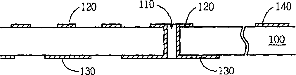
[0033] Please refer to Figure 2A to Figure 2I , which shows a schematic diagram of a preferred embodiment of the manufacturing method of the packaging substrate of the present invention. First, if Figure 2A As shown, on a core substrate (Core Substrate) 200 , through-holes are made through the core substrate 200 mechanically or by laser. Subsequently, a plated through hole (Plated Through Hole, PTH) 210 is formed in the through hole by electroplating, and, on the upper and lower sides of the core substrate 200 , wire layers 202 are respectively formed to connect to the through hole 210 .

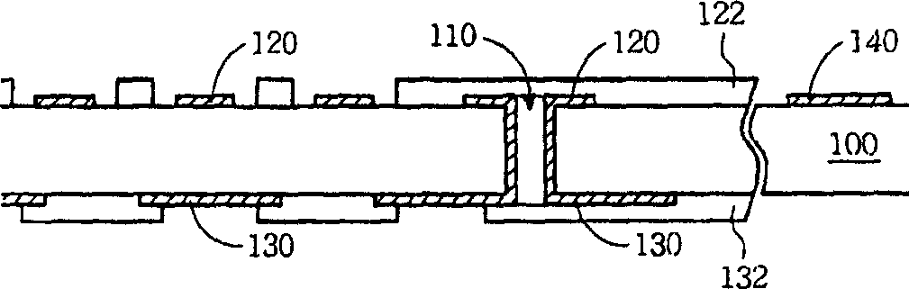
[0034] Next, if Figure 2B As shown, the conductive layer 202 is lithographically etched to form the first conductive pattern layer 220 and the second conductive pattern layer 230 on the upper and lower surfaces of the core substrate 200, and the first conductive pattern layer 220 passes through the via hole 210 is connected to the second wire pattern layer 230 to form a circuit substra...


PUM


Abstract

A seal substrate and its manufacture method, includes wire pattern made on upper and lower planes of circuit substrate and connected to each other. Melting-resistant layer is created on the uncovered plane of wire pattern to limit the position of junction on upper and lower planes of seal substrate, then, solder layer is filled in the opening of melting-resistant layer on the lower plane to finish capsulation to the junction of lower plane. Conducting seed crystal layer is made on the lower plane , and on whose lower plane protective film is made, then, steps of electroplate is operated for making mantel on the junction of upper plane of seal substrate.

Description

technical field [0001] The invention relates to a packaging substrate and a manufacturing method thereof, in particular to a packaging substrate of an electroless plating bar (Plating Bar) and a manufacturing method thereof. Background technique [0002] With the rapid development of semiconductor technology, there are requirements for processor miniaturization, multi-functionality and processing speed. In order to meet this requirement, the number of connection points (I / O) of the processor must first be increased to meet the processing requirements of multi-function signals. A typical solution is to change the configuration of the connection points, so that the low-density surrounding distribution method is transformed into a high-density matrix distribution (Array Pad) method. At the same time, in order to cooperate with the high-density matrix distribution (Pitch≤200μm) connection point configuration method, the packaging technology of the processor has also developed f...

Claims


Application Information

Patent Timeline
IPC IPC(8): H01L21/48H05K3/00
Inventor 何昆耀宫振越
Owner VIA TECH INC
Why Eureka
Try Eureka