Process for forming a patterned thin film structure for in-mold decoration

A technology for patterning thin films and thin film structures, applied in chemical instruments and methods, removing conductive materials by mechanical methods, display devices, etc., can solve problems such as expensive, environmental hazards, and time-consuming

Inactive Publication Date: 2005-03-23
SIPIX CHEM
View PDF0 Cites 37 Cited by
  • Summary
  • Abstract
  • Description
  • Claims
  • Application Information

AI Technical Summary

Problems solved by technology

[0005] Certain process steps in photolithographic methods, such as pattern exposure, are time-consuming and require careful registration and alignment of the mask and the moving target area
Additionally, developing and removing photoresist and disposing of waste from the chemical etching process can be time-consuming and expensive, in addition to potentially causing environmental hazards
Chemical etching methods also tend to result in a less glossy surface, which is often undesirable for high-end decorative applications

Method used


Image

  • Process for forming a patterned thin film structure for in-mold decoration
  • Process for forming a patterned thin film structure for in-mold decoration
  • Process for forming a patterned thin film structure for in-mold decoration

Examples


Embodiment Construction

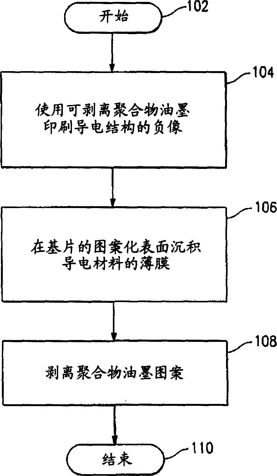
[0082] Detailed descriptions of preferred embodiments of the invention are provided below. While the invention has been described in connection with preferred embodiments, it is to be understood that the invention is not limited to any one particular embodiment. On the contrary, the scope of the invention is limited only by the claims and the invention encompasses numerous alternatives, modifications, and equivalents. In the following description, for purposes of illustration and description, numerous specific details are given in order to provide a thorough understanding of the invention. The invention may be practiced in accordance with the scope without some or all of these specific details. For the purpose of clarity, technical material that is known in the technical fields related to the invention has not been described in detail so as not to obscure the content of the invention.

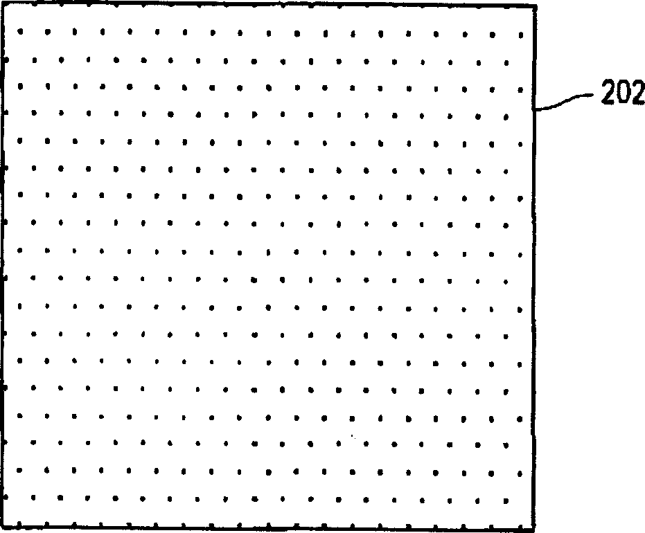
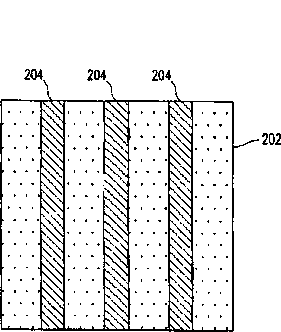
[0083] The invention discloses a method for forming a patterned thin film structure on a ...


PUM

PropertyMeasurementUnit
thicknessaaaaaaaaaa
thicknessaaaaaaaaaa
thicknessaaaaaaaaaa

Abstract

A process for forming a patterned thin film structure on a substrate or in-mold decoration film is disclosed. A pattern is printed with a material, such as a masking coating or ink, on the substrate, the pattern being such that, in one embodiment, the desired structures will be formed in the areas where the printed material is not present, i.e., a negative image of thin film structure to be formed is printed. In another embodiment, the pattern is printed with a material that is difficult to strip from the substrate, and the desired thin film structures will be formed in the areas where the printed material is present, i.e., a positive image of the thin film structure is printed. The thin film material is deposited on the patterned substrate, and the undesired area is stripped, leaving behind the patterned thin film structure.

Description

technical field [0001] The present invention relates generally to in-mold decoration. The invention discloses a method for forming a patterned thin film on a substrate for in-mold decoration. Background technique [0002] In-mold decoration (IMD) has emerged as an increasingly popular set of techniques for decorating injection molded parts. IMD technology is used to add text, numbers, legends, other symbols and information, and purely decorative designs to injection molded parts such as telephones and other consumer electronic devices, automotive dashboards, containers and packaging materials for consumer products, And in fact the whole field of injection molded parts. [0003] IMD generally involves forming an in-mold decoration film (IMD film or IMD decoration film) that includes an image to be transferred to or bonded to the surface of an injection molded part. In a typical in-mold transfer method, a polyethylene terephthalate (PET) film is treated with a release agent...

Claims


Application Information

Patent Timeline
Patent Type & Authority Applications(China)
IPC IPC(8): B29CB41M1/30C23C14/04C23C14/08C23C14/20G02F1/1343H01L51/00H05K3/04H05K3/14H05K3/16H05K3/18H05K3/38
CPCH01L51/0022H05K2201/0317H05K3/184C23C14/086H05K2203/0257H05K3/146H05K3/048H05K2203/0264Y10S156/922B32B38/10C23C14/20C23C14/042H05K3/16H05K2203/0522H05K2203/0746H05K3/04H05K3/386B29K2995/002B29C45/14811G09F7/165G02F1/13439Y10T156/1189Y10T156/11H10K71/611
Inventor 赵一雄张小加史恩·奇拉克曾金仁臧宏玫梁荣昌
Owner SIPIX CHEM
Why Eureka
Try Eureka