Thin film transistor array

A technology of thin film transistors and data wiring, applied in transistors, optics, instruments, etc., can solve problems such as capacitor leakage, achieve the effects of increasing storage capacitors, high display quality, and reducing the probability of capacitor leakage

Inactive Publication Date: 2005-03-23
AU OPTRONICS CORP
View PDF0 Cites 13 Cited by
  • Summary
  • Abstract
  • Description
  • Claims
  • Application Information

AI Technical Summary

Problems solved by technology

[0008] The purpose of the present invention is to provide a thin film transistor array, which can improve the problem of capacitance leakage caused by particle pollution, and increase the storage capacitance without affecting the aperture ratio and the reliability of the transistor components, so as to improve the performance of the liquid crystal panel

Method used


Image

  • Thin film transistor array
  • Thin film transistor array
  • Thin film transistor array

Examples


Embodiment Construction

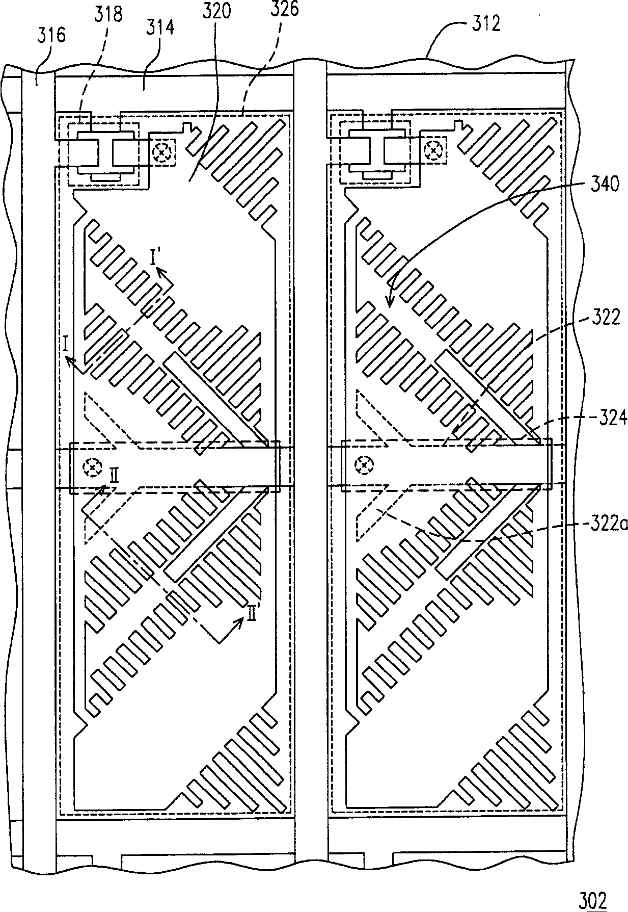
[0038] The present invention increases the storage capacitance through the shared wiring with branches, and the branches of these shared wirings correspond to the parts with poor luminous efficiency in the pixel area, so the influence on the aperture ratio of the pixel structure can be reduced. The following examples will be given to illustrate the present invention, but they are not intended to limit the present invention. Those skilled in the art can make appropriate modifications to the following examples according to the spirit of the present invention, but still fall within the scope of the present invention.

[0039]The thin film transistor array of the present invention can form a Multi-Domain Vertical Alignment (MVA) liquid crystal display panel together with a known and suitable color filter and a known and suitable liquid crystal layer. Generally speaking, the color filter of a traditional multi-domain vertically aligned liquid crystal display panel is mainly composed...


PUM


Abstract

The invention discloses a film transistor array, which has several shared wirings to provide storing capacitance for pixel. Especially, each shared wiring has several branched wirings. The shared wiring and the branched wirings constitutes storing capacitance with pixel electrode. The branched wirings are located at the poor light efficiency spots of a pixel area, so the pixel storing capacitance can be increased when the pixel uncork ratio is not influenced, and the efficiency of liquid crystal panel can be improved.

Description

technical field [0001] The present invention relates to a display device, and in particular to a thin film transistor array capable of increasing storage capacity. Background technique [0002] The rapid progress of the multimedia society is mostly due to the dramatic progress of semiconductor components or display devices. As far as displays are concerned, thin film transistor liquid crystal displays (Thin FilmTransistor Liquid Crystal Display, TFT-LCD) with superior characteristics such as high image quality, good space utilization efficiency, low power consumption, and no radiation have gradually become the mainstream of the market. [0003] A thin film transistor liquid crystal display (TFT-LCD) is mainly composed of a thin film transistor array, a color filter and a liquid crystal layer. The thin film transistor array is composed of a plurality of thin film transistors arranged in an array and a pixel electrode (pixel electrode) corresponding to each thin film transist...

Claims


Application Information

Patent Timeline
Patent Type & Authority Applications(China)
IPC IPC(8): G02F1/133G02F1/136H01L29/786
Inventor 来汉中
Owner AU OPTRONICS CORP
Why Eureka
Try Eureka