Semiconductor device and manufacturing method thereof
一种制造方法、半导体的技术,应用在半导体/固态器件制造、半导体器件、半导体/固态器件零部件等方向,能够解决芯片变薄强度弱、位置精度变低、半导体芯片破裂等问题
- Summary
- Abstract
- Description
- Claims
- Application Information
AI Technical Summary
Problems solved by technology
Method used
Image

Examples
Embodiment Construction
[0048] Embodiments of the present invention are described with reference to the drawings.
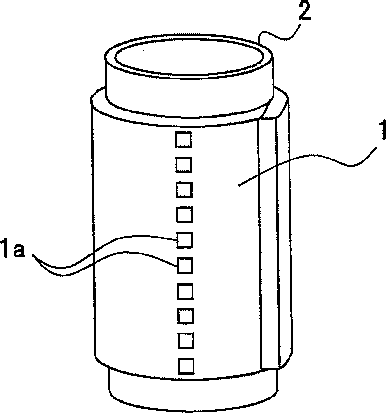
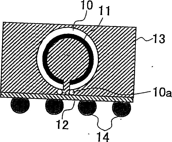
[0049] image 3 It is a sectional view of the semiconductor device according to the first embodiment of the present invention. image 3 The shown semiconductor device has a semiconductor chip 10 bent into a substantially cylindrical shape. The bumps 10 a serving as external connection terminals in the semiconductor chip 10 are bent outward. The bumps 10a are formed of solder or gold. The bumps 10 a arranged around both sides of the semiconductor chip 10 are aligned in two rows in the longitudinal direction of the cylindrical shape. On the back surface (cylindrical inner surface) of the semiconductor chip 10, a coating material 11 such as resin as a fixing member is applied and cured to form a resin layer. In this way, the semiconductor chip is fixed by the resin layer in a state of being bent into a cylindrical shape.
[0050] The semiconductor chip 10 is connected to a package sub...
PUM
 Abstract
Description
Claims
Application Information
 - R&D
- Intellectual Property
- Life Sciences
- Materials
- Tech Scout
- Unparalleled Data Quality
- Higher Quality Content
- 60% Fewer Hallucinations
Browse by: Latest US Patents, China's latest patents, Technical Efficacy Thesaurus, Application Domain, Technology Topic, Popular Technical Reports.
© 2025 PatSnap. All rights reserved.Legal|Privacy policy|Modern Slavery Act Transparency Statement|Sitemap|About US| Contact US: help@patsnap.com