Circuit component module and method of manufacturing the same

A technology of circuit components and manufacturing methods, which is applied in the direction of printed circuit manufacturing, multilayer circuit manufacturing, and electric circuits, can solve problems such as poor conduction, insufficient contact, and reduced precision of finishing, so as to reduce the possibility of being etched and prevent Reduction of line width and improvement of bonding strength

Inactive Publication Date: 2005-10-05
ALPS ALPINE CO LTD
View PDF4 Cites 4 Cited by
  • Summary
  • Abstract
  • Description
  • Claims
  • Application Information

AI Technical Summary

Problems solved by technology

[0009] However, in the circuit component module described in Patent Document 1, contact holes for wiring are formed after the organic polymer is applied by roll coating or the like after the components are arranged, and then fired, so that the unevenness of the resin surface cannot be ensured well. The precision of the joint of the parts due to
In addition, there is a problem that poor conduction due to resin residue on the die pad or damage to the junction due to stress generated between the component and the resin is likely to occur.
[0010] In addition, even the circuit component module described in Patent Document 2 has a problem that damage to joints is likely to occur due to heat and stress in the manufacturing process.
Furthermore, since it is necessary to go through the process of aligning the patterns with each other many times, there is a problem that it is easy to cause a decrease in the precision of the finishing process and increase the manufacturing cost.
[0011] Also, in the circuit board described in Patent Document 3, when the copper foils are crimped on both sides of the dielectric substrate by current heating or the like, the dielectric substrate softens in advance and adheres to the copper foils, and then softens in the through-hole. The metal particle-doped resin filled in the hole, the contact between the metal particle-doped resin and the copper foil becomes insufficient, which may reduce the reliability
[0012] Furthermore, as in the case of Patent Document 3, the circuit board described in Patent Document 4 is also the same. The dielectric material constituting the circuit board softens earlier than the conductive resin, and the contact between the conductive resin and the metal film becomes insufficient, which may cause the decreased reliability

Method used


Image

  • Circuit component module and method of manufacturing the same
  • Circuit component module and method of manufacturing the same
  • Circuit component module and method of manufacturing the same

Examples


no. 1 example

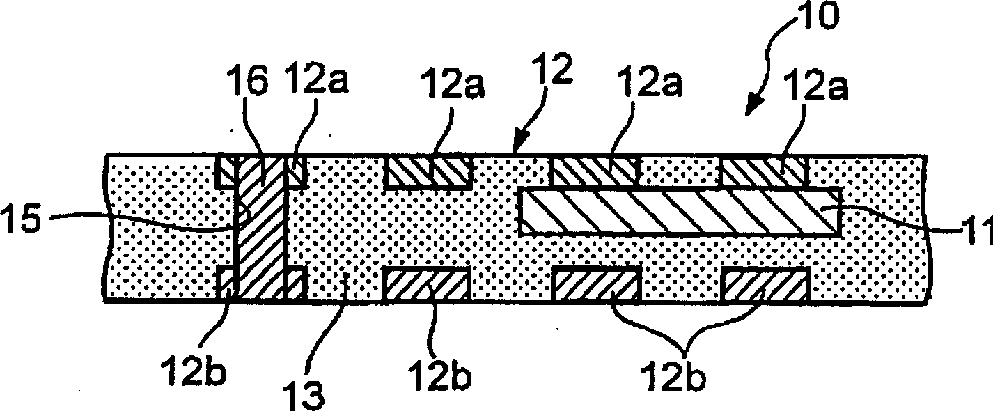
[0048] Next, a first embodiment of the present invention will be described with reference to the drawings. figure 1 It is a sectional view showing an example of the circuit component module of the first embodiment of the present invention. For example, the circuit component module 10 is a thin plate-shaped component-mounted circuit board with an overall thickness of about 0.3 mm. The circuit component module 10 has electronic components 11 , wiring 12 formed in a predetermined pattern, and a resin layer 13 covering part of these electronic components 11 and wiring 12 .

[0049] Wiring 12 includes first wiring 12 a and second wiring 12 b formed to face each other via resin layer 13 , and may be made of, for example, Cu or the like. The first wiring 12a or the second wiring 12b is connected to the electronic component 11 at a predetermined position.

[0050] For example, the resin layer 13 may be formed of an insulating thermosetting resin. Furthermore, a hole 15 is formed in...

no. 2 example

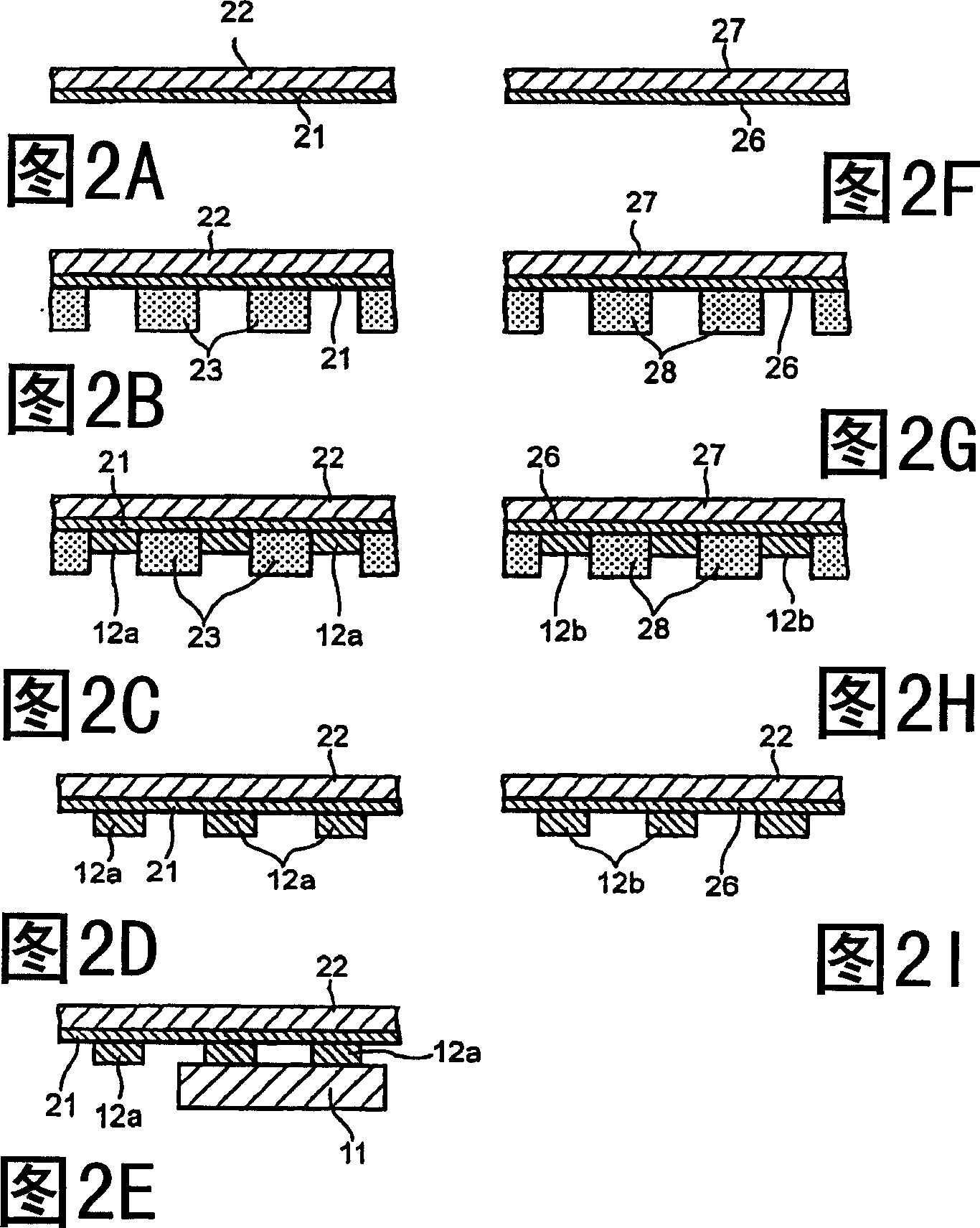
[0062] Next, an electronic component module and a manufacturing method thereof according to a second embodiment of the present invention will be described.

[0063] The method of manufacturing an electronic component module according to this embodiment includes a wiring forming step of forming a wiring portion on a flat substrate, a resin layer forming step, a crimping step of embedding the wiring portion in the resin layer and bonding it under pressure, and a step of peeling the flat substrate from the resin layer. Schematic configuration of the peeling process. Hereinafter, each step will be described with reference to the drawings. 5 to 8 show process diagrams of the method of manufacturing the electronic component module of the present embodiment. In addition, these figures are for explaining the electronic component module of this embodiment and its manufacturing method, and the size, thickness, dimension, etc. of each part shown in a figure do not necessarily correspond...

no. 3 example

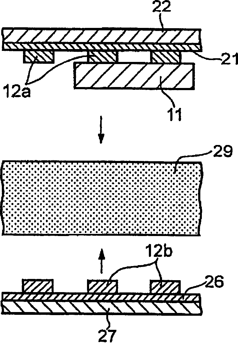
[0094] Next, an electronic component module and a manufacturing method thereof according to a third embodiment of the present invention will be described.

[0095] The manufacturing method of the electronic component module of this embodiment is the same as that of the second embodiment, including the wiring forming step of forming the wiring portion on the flat substrate, the resin layer forming step, the crimping step of embedding the wiring portion in the resin layer and crimping it, Schematic configuration of the peeling process for peeling the flat substrate from the resin layer. Next, each step will be described with reference to the drawings. 9 to 12 show process diagrams of the method of manufacturing the electronic component module of the present embodiment. In addition, these figures are for explaining the electronic component module of this embodiment and its manufacturing method, and the size, thickness, dimension, etc. of each part shown in a figure do not necess...


PUM


Abstract

The present invention provided a circuit component module having high precision, reliability, and low manufacturing cost, and to provide a manufacturing method of the module. The circuit component module 10 is provided with an electronic component 11, a wiring line 12 formed by a prescribed pattern and a resin layer 13 covering a part of the electronic component 11 and the wiring line 12. The wiring line 12 is composed of a first wiring line 12a and a second wiring line 12b which are formed mutually facing via the resin layer 13, and it can be composed of Cu and the like, for example. The first wiring line 12a and the second wiring line 12b are connected to the electronic component 11 at prescribed positions.

Description

technical field [0001] The present invention relates to a thin and light circuit component module incorporating various electronic components and a manufacturing method thereof. Background technique [0002] For example, in portable electronic devices such as mobile phones and PDAs, thin-plate-shaped circuit component modules integrating circuit boards and various components are being used in order to reduce size, weight and cost. For example, as shown in Patent Document 1 or Patent Document 2, such a circuit component module is a module in which various components are embedded in a substrate such as resin and a conductive circuit pattern is formed on the surface, and it is formed in a flat plate shape with few unevenness and is thin. It is light in weight and excellent in mass productivity, so it is suitable as a component substrate for portable electronic devices that require downsizing and weight reduction. [0003] In addition, Patent Document 3 discloses that a through...

Claims


Application Information

Patent Timeline
Patent Type & Authority Applications(China)
IPC IPC(8): H01L23/02H01L23/538H05K1/18H05K3/00H05K3/20H05K3/40H05K3/46
CPCH05K3/205H05K2203/095H01L23/5389H01L2224/16H01L2924/01078H01L2924/01079H01L23/5384H05K1/187H05K3/4069H01L2224/05568H01L2224/05573H01L2924/00014H01L2224/05599
Inventor 佐佐木顺彦松桥清
Owner ALPS ALPINE CO LTD
Why Eureka
Try Eureka