Supercharge Your Innovation With Domain-Expert AI Agents!

Minitype EEPROM matrix structure

A technology of read-only memory and matrix structure, which is applied in read-only memory, static memory, information storage, etc., can solve the problems that the effective bit unit of EEPROM cannot be reduced, and the area is large, so as to improve the integration The effect of reducing the size, reducing the area and reducing the width

Inactive Publication Date: 2005-11-02
SEMICON MFG INT (SHANGHAI) CORP
View PDF0 Cites 0 Cited by
  • Summary
  • Abstract
  • Description
  • Claims
  • Application Information

AI Technical Summary

Problems solved by technology

Each control grid (CG) and signal grid in the existing EEPROM have connection joints respectively, therefore, the occupied area is large, thus can not reduce the final effective bit unit of the electrically erasable programmable read-only memory (EEPROM) matrix

Method used


Image

  • Minitype EEPROM matrix structure
  • Minitype EEPROM matrix structure
  • Minitype EEPROM matrix structure

Examples


Embodiment Construction

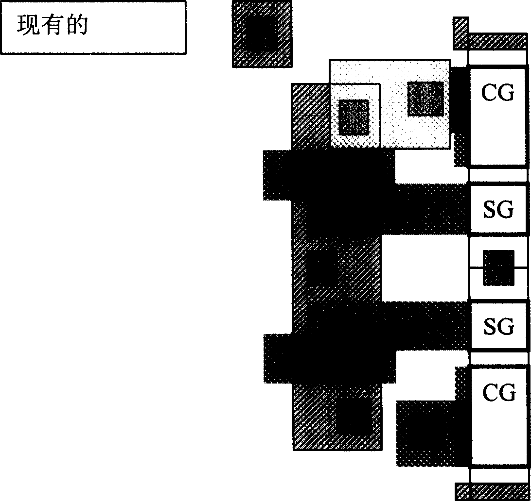
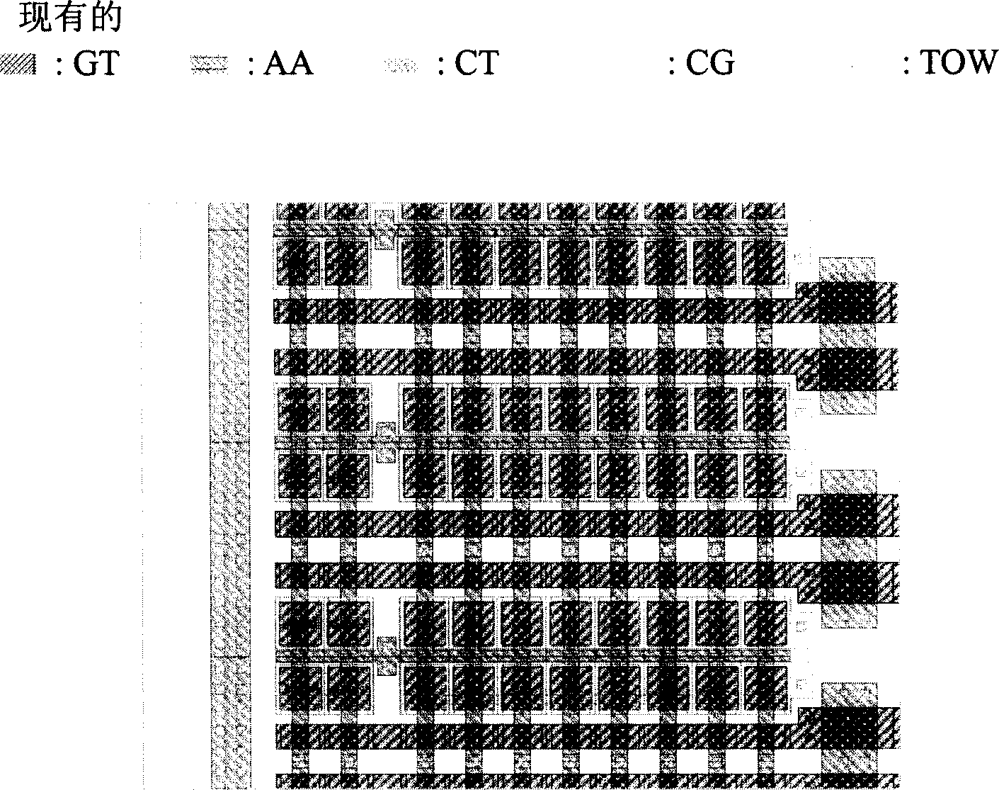
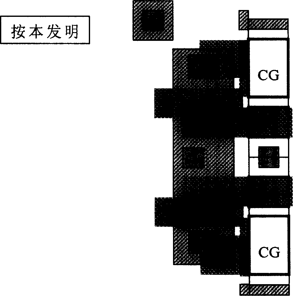
[0015] figure 1 It is a schematic diagram illustrating the matrix structure of the existing electrically erasable programmable read-only memory. figure 2 It is a schematic diagram illustrating the layout of signal gate-signal gate contacts in the existing EEPROM matrix structure. image 3 Is to illustrate the electrical erasable programmable read-only memory matrix structure according to the present invention pair Signal Grid Layout- pair Schematic diagram of a junction with enlarged signal bars. Figure 4 It is a partially enlarged schematic diagram illustrating the dual signal gate layout-enlarged dual signal gate contacts in the EEPROM matrix structure of the present invention. and Figure 5 It is a schematic diagram illustrating the dual signal gate layout-double signal gate enlarged contacts in the EEPROM matrix structure of the present invention.

[0016] Referring now to the accompanying drawings, describe in detail the matrix structure of the small electrically...


PUM


Abstract

The invention provides a matrix structure for EEPROM, which comprises multiple EPROM and is characterized in that every EEPROM uses butted CT to connect adjacent two signal grids; as EEcell, the butted CT decreases CG size and can constitute less EEPROM effective bitcell. Compared with existing integrated level of EEPROM matrix, the integrated level by this invention can increase 5%~15%.

Description

technical field [0001] The invention relates to a small semiconductor device, in particular to an electrically erasable programmable read-only memory matrix structure. Background technique [0002] Improving the electrical performance of electronic products and reducing the volume and weight of electronic products are the goals that people are constantly pursuing. Miniaturizing semiconductor devices and improving the integration of integrated circuits are extremely important tasks in achieving this goal. [0003] In order to improve the integration of integrated circuits, the area occupied by each component must be as small as possible, the size of each component that constitutes a semiconductor device must be as small as possible, and the layout of each component that constitutes a semiconductor device must be as small as possible. compact. [0004] As far as the final effective bit cells of the Electrically Erasable Programmable Read Only Memory (hereinafter referred to ...

Claims


Application Information

Patent Timeline
Patent Type & Authority Applications(China)
IPC IPC(8): G11C16/02
Inventor 詹奕鹏刘梅
Owner SEMICON MFG INT (SHANGHAI) CORP
Features
  • R&D
  • Intellectual Property
  • Life Sciences
  • Materials
  • Tech Scout
  • Unparalleled Data Quality
  • Higher Quality Content
  • 60% Fewer Hallucinations
Learn More