Solid-state imaging device, semiconductor wafer and camera module

A camera device, solid-state technology, applied in semiconductor devices, electric solid-state devices, radiation control devices, etc., to achieve the effect of reducing adverse effects

Inactive Publication Date: 2005-12-07
SHARP KK
View PDF4 Cites 5 Cited by
  • Summary
  • Abstract
  • Description
  • Claims
  • Application Information

AI Technical Summary

Problems solved by technology

Furthermore, the problem of defects caused by impurity mixing or impurity adhesion also occurs in films other than these examples, and the film forming method is not limited to the physical vapor deposition method. Problems caused by contamination of impurities or adhesion of impurities

Method used


Image

  • Solid-state imaging device, semiconductor wafer and camera module
  • Solid-state imaging device, semiconductor wafer and camera module
  • Solid-state imaging device, semiconductor wafer and camera module

Examples


Embodiment approach 1

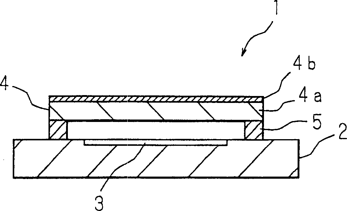
[0028] figure 1 is a cross-sectional view showing the configuration of the solid-state imaging device of the present invention. The solid-state imaging device 1 includes: a solid-state imaging element 2 formed in a rectangular shape in plan view on a semiconductor substrate; a light-receiving unit 3 formed on one surface of the solid-state imaging element 2; and on one side of the solid-state imaging device 2, a bonding portion 5 for bonding the light-transmitting cover portion 4 and the solid-state imaging device 2 is formed in a region except the light receiving portion 3. The solid-state imaging device 1 takes in light from the outside through the translucent cover portion 4 , and receives the light through the light-receiving elements (effective pixels) arranged on the light-receiving portion 3 of the solid-state imaging device 2 . In addition, although not shown in the figure, microlenses are arranged on the surface of the light receiving unit 3 to converge incident ligh...

Embodiment approach 2

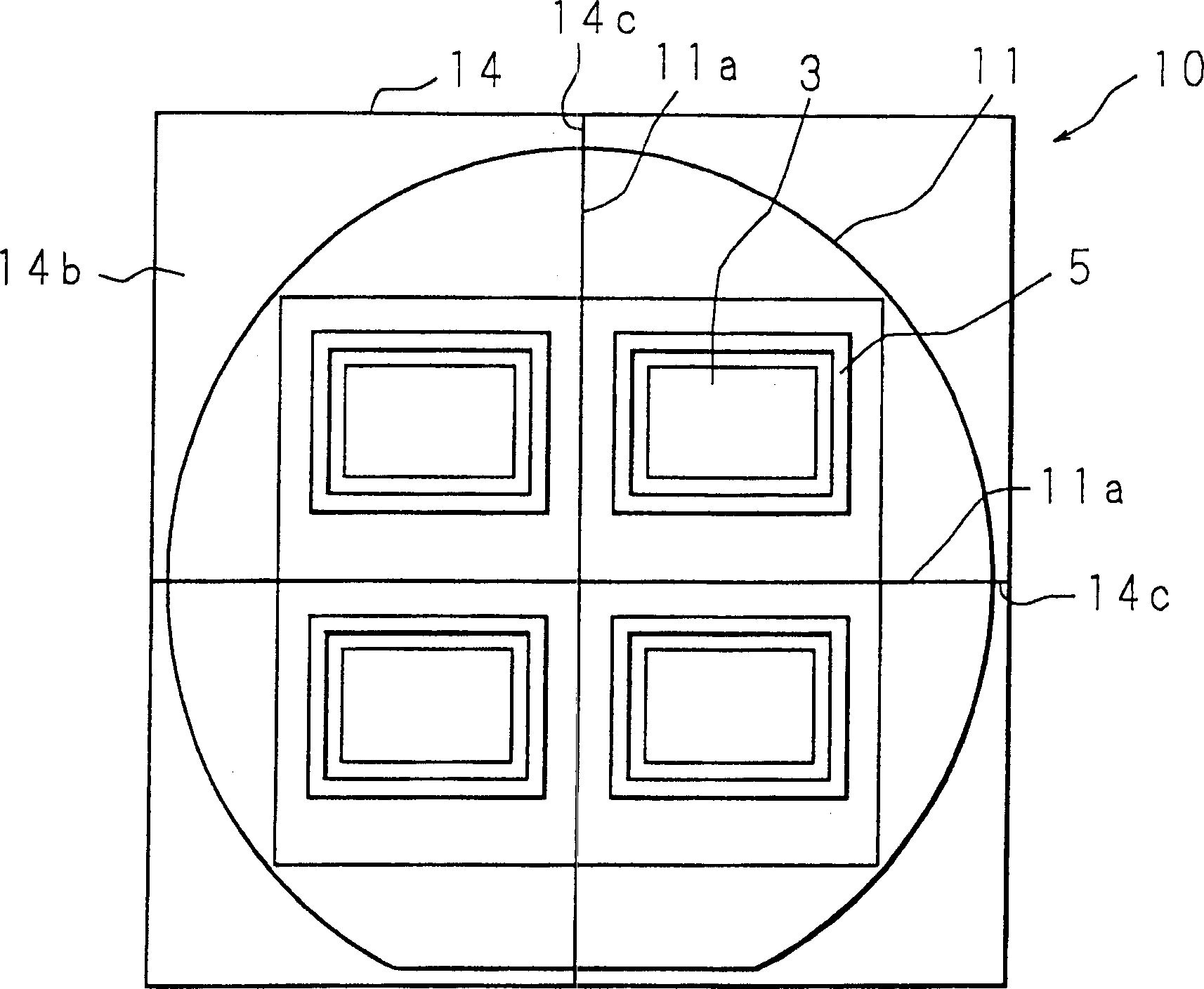
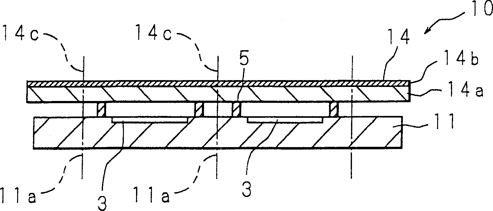
[0034] Figure 2A and 2B shows the structure of an example of the semiconductor wafer of the present invention, Figure 2A is its top view, Figure 2B is its cross-section. The semiconductor wafer 10 has a structure in which a light-transmitting plate 14 is bonded via an adhesive portion 5 to a semiconductor substrate 11 on which a plurality of light receiving portions 3 are patterned on one surface. In addition, although not shown in the figure, microlenses are arranged on the surface of the light receiving unit 3 to converge incident light on the light receiving element of each pixel.

[0035] The translucent plate 14 is made of a glass substrate 14a and an infrared shielding film 14b formed on one side of the glass substrate 14a, and the translucent plate 14 is arranged so that the one side of the translucent plate 14 (glass substrate 14a) on which the infrared shielding film 14b is formed It becomes the side opposite to the side of the semiconductor substrate 11 that f...

Embodiment approach 3

[0041] Figure 3A And 3B has shown the structure of other examples of the semiconductor wafer of the present invention, Figure 3A is its top view, Figure 3B is its cross-section. The semiconductor wafer 20 has a structure in which a plurality of singulated light-transmitting cover portions 4 are bonded by bonding portions 5 on a semiconductor substrate 11 on which a plurality of light receiving portions 3 are patterned on one surface. In addition, although not shown in the figure, microlenses are arranged on the surface of the light receiving unit 3 to converge incident light on the light receiving element of each pixel.

[0042] Each light-transmitting cover portion 4 is the same as the light-transmitting cover portion 4 of the first embodiment, and each light-transmitting cover portion 4 is arranged such that each light-transmitting cover portion 4 (each glass substrate 4 a ) on which an infrared shielding film 4 b is formed One side is the side opposite to the side fac...


PUM


Abstract

A light-permeable lid provided oppositely to a photodetector of a solid-state imaging element includes a glass substrate, and an infrared-ray shielding film formed on one side of the glass substrate. The light-permeable lid is disposed so that the side of the light-permeable lid (glass substrate) forming the infrared-ray shielding film is positioned at the opposite side of the side facing the photodetector of the solid-state imaging element. If dust mixes in the infrared-ray shielding film or dust deposits to the film, since the distance from the photodetector to dust (infrared-ray shielding film) is longer, the photodetector is less susceptible to adverse influence of the dust and occurrence of defect due to the dust can be decreased.

Description

technical field [0001] The present invention relates to a solid-state imaging device such as a CCD or a C-MOS imager used for imaging in a mobile phone, a semiconductor wafer used in the manufacture of the solid-state imaging device, and a camera module using the solid-state imaging device. Background technique [0002] A solid-state imaging device used in a compact camera attached to a mobile phone includes a solid-state imaging element having a light-receiving portion. In such a solid-state imaging element, for the purpose of protecting the light-receiving portion, the general structure is that the solid-state imaging element is made of glass or the like with an adhesive. The formed light-transmitting cover portion is bonded to the semiconductor substrate (see, for example, JP-A-7-202152, JP-A-2001-351997, and JP-A-2003-197656). The translucent cover protects the surface of the light receiving unit from impurities, scratches, and the like. [0003] In ...

Claims


Application Information

Patent Timeline
Patent Type & Authority Applications(China)
IPC IPC(8): H01L27/14H01L31/0203H04N5/225H04N5/335H04N5/372H04N5/374
CPCH01L27/14627H01L27/14621H01L27/14649H01L27/14618H01L2224/48091H01L2924/16235H01L2924/00014H01L27/146
Inventor 内田健治
Owner SHARP KK
Why Eureka
Try Eureka