Plasma processing apparatus and plasma processing method

A plasma and processing device technology, applied in the field of plasma processing devices, can solve the problems of substrate degradation, transistor characteristic degradation, leakage current increase, etc.

Inactive Publication Date: 2005-12-28
TOKYO ELECTRON LTD
View PDF0 Cites 2 Cited by
  • Summary
  • Abstract
  • Description
  • Claims
  • Application Information

AI Technical Summary

Problems solved by technology

Due to the damage of the film, problems such as deterioration of the substrate, increase in leakage current, and deterioration of transistor characteristics due to deterioration of interface characteristics may occur.
[0004] In addition, as another problem, there is a problem that the film thickness of the silicon nitride film increases more than necessary due to the diffusion of oxygen element to the interface between the silicon oxide film and the silicon nitride film.

Method used


Image

  • Plasma processing apparatus and plasma processing method
  • Plasma processing apparatus and plasma processing method
  • Plasma processing apparatus and plasma processing method

Examples


Embodiment Construction

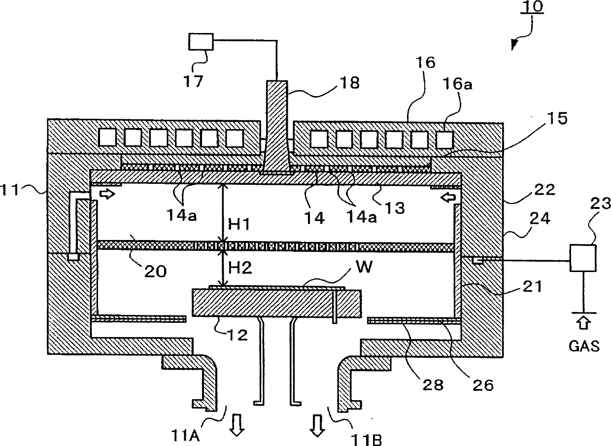
[0021] FIG. 1 shows a schematic configuration of a plasma processing apparatus 10 according to an embodiment of the present invention. The plasma processing apparatus 10 has a processing container 11 formed with a substrate holding table 12 holding a silicon wafer W as a substrate to be processed, and air (gas) in the processing container 11 is exhausted through exhaust holes 11A, 11B. In addition, the substrate holding table 12 has a heater function for heating the silicon wafer W. As shown in FIG.

[0022] An opening corresponding to the silicon wafer W on the substrate holding table 12 is formed above the processing container 11 . The opening is made of quartz and Al 2 o 3 The formed dielectric plate 13 is plugged. A slot plate 14 functioning as an antenna is disposed on (outside) the dielectric plate 13 . The slot plate 14 is made of a conductive material such as a thin circular plate of copper, and a plurality of long holes 14a are formed. These elongated holes 14a a...


PUM

PropertyMeasurementUnit
areaaaaaaaaaaa
thicknessaaaaaaaaaa
diameteraaaaaaaaaa

Abstract

According to the present invention, when nitriding the surface of the silicon substrate, a spacer having an opening is arranged between the plasma generating part and the silicon substrate, and the electron density on the surface of the silicon substrate is controlled to be 1e+7 (unit·cm-3) ~1e+9 (unit cm-3). According to the present invention, deterioration of the silicon substrate and the nitride film is effectively suppressed.

Description

technical field [0001] The present invention relates to a plasma processing device and a plasma processing method for nitriding or oxidizing a silicon substrate using plasma. Background technique [0002] When nitriding a silicon substrate using plasma, for example, nitrogen gas or nitrogen gas and hydrogen gas, or NH 3 A gas containing nitrogen element such as gas. As a result, N radicals or NH radicals are generated to convert the surface of the silicon oxide film into a nitride film. In addition, there is also a method of directly nitriding the surface of a silicon substrate by microwave plasma. [0003] According to the existing devices and methods, due to the ions incident on the silicon oxide mold (silicon substrate), the base film (Si, SiO 2 ) or the problem that the formed film (SiN) is damaged. Damage to the film may cause problems such as degradation of the substrate, increase in leakage current, and degradation of transistor characteristics due to degradation ...

Claims


Application Information

Patent Timeline
Patent Type & Authority Applications(China)
IPC IPC(8): C23C8/36C23C16/00H01L21/314H01L21/316H01L21/318H01L21/321
CPCC23C8/36H01L21/3211H01L21/02238H01L21/02164H01L21/02252H01L21/0217H01L21/3144H01L21/31662H01L21/3185H01L21/0234H01L21/02332
Inventor 中西敏雄西田辰夫尾崎成则
Owner TOKYO ELECTRON LTD
Why Eureka
Try Eureka