Optical assembly packaging structure and mfg. method thereof
A technology of optical components and manufacturing methods, which is applied in the field of packaging structure, can solve the problems of expensive ceramic substrates, etc., and achieve the effects of reducing manufacturing costs, preventing moisture, and reducing deflection
- Summary
- Abstract
- Description
- Claims
- Application Information
AI Technical Summary
Problems solved by technology
Method used
Image

Examples
Embodiment Construction
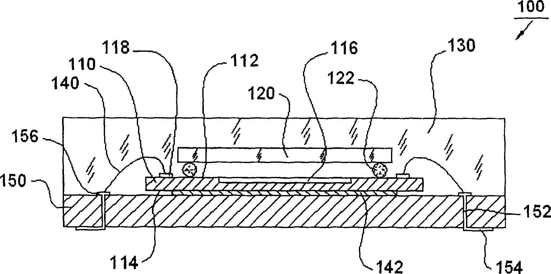
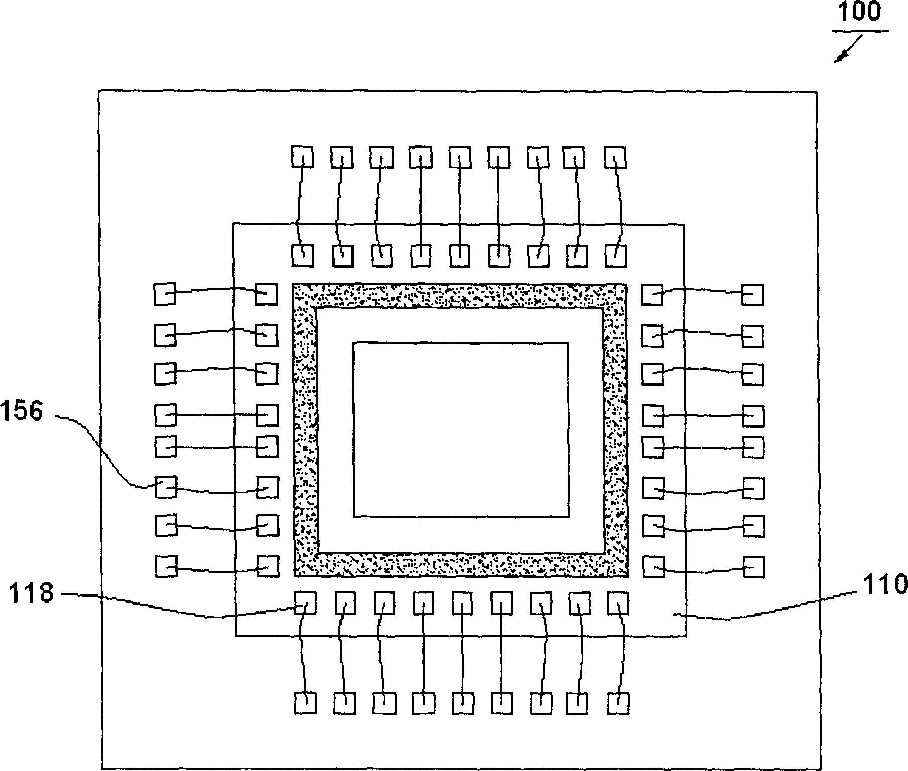
[0013] Please refer now figure 1 , which shows an optical component packaging structure 100 according to an embodiment of the present invention. The package structure 100 includes a chip 110 having an active surface 112 and an opposite back surface 114. The active surface 112 of the chip 110 has an active zone 116 having a plurality of optical components, such as optical sensors. , for conversion between optical and electrical signals.
[0014] A sealant 122 is disposed on the active surface 112 of the chip 110 around the optical component 114 . A cover 120 is disposed on the sealant 122 , and is adhered and fixed on the chip 110 by the sealant 122 . The sealant 122 is mixed with a spacer (not shown in the figure), so that a certain gap is maintained between the outer cover 120 and the chip 110 . Furthermore, the outer cover 120 may be a simple transparent outer cover. Alternatively, the outer cover 120 can be used to provide optical properties, such as filter and focusing...
PUM
 Abstract
Description
Claims
Application Information
 - Generate Ideas
- Intellectual Property
- Life Sciences
- Materials
- Tech Scout
- Unparalleled Data Quality
- Higher Quality Content
- 60% Fewer Hallucinations
Browse by: Latest US Patents, China's latest patents, Technical Efficacy Thesaurus, Application Domain, Technology Topic, Popular Technical Reports.
© 2025 PatSnap. All rights reserved.Legal|Privacy policy|Modern Slavery Act Transparency Statement|Sitemap|About US| Contact US: help@patsnap.com