Manufacturing system

A technology of manufacturing system and control device, applied in manufacturing tools, semiconductor/solid-state device manufacturing, control of workpiece feed movement, etc., can solve problems such as adjustment of grinding amount, and achieve the effect of improving flattening effect

Inactive Publication Date: 2006-03-08
TAIWAN SEMICON MFG CO LTD
View PDF0 Cites 9 Cited by
  • Summary
  • Abstract
  • Description
  • Claims
  • Application Information

AI Technical Summary

Problems solved by technology

The second grinding process removes copper remaining on the substrate, but the amount of grinding is not adjusted based on the results of the first grinding process

Method used


Image

  • Manufacturing system
  • Manufacturing system
  • Manufacturing system

Examples


Embodiment Construction

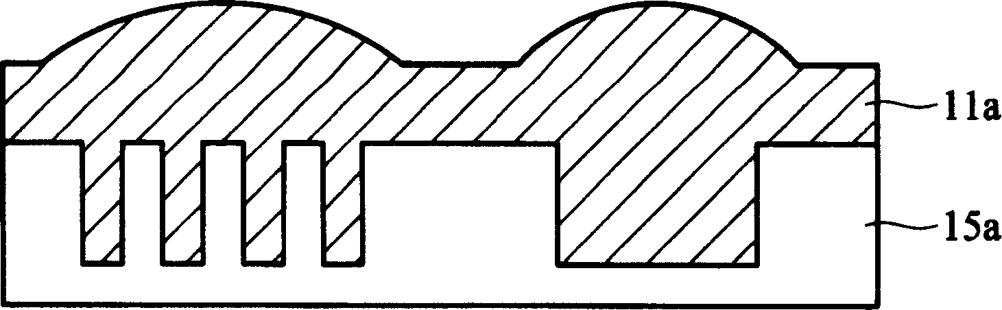
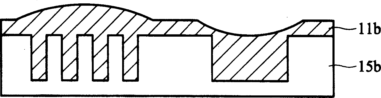
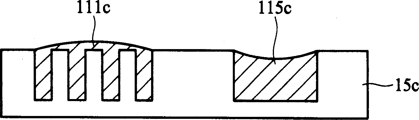
[0025] In order to make the purpose, features, and advantages of the present invention more obvious and easy to understand, the preferred embodiments are specifically cited below, together with the attached figure 2 to attach Figure 6 , give a detailed explanation. The description of the present invention provides different examples to illustrate the technical features of different implementations of the present invention. Wherein, the configuration of each element in the embodiment is for illustration, not for limiting the present invention. In addition, the reference numerals in the embodiments are partly repeated for the purpose of simplifying the description, and do not imply the correlation between different embodiments.

[0026] The present invention takes the CMP process of removing copper film as an example, but the application of the present invention is not limited thereto. Other metal film removal processes are performed in a face-down (face-down) manner during ...


PUM


Abstract

A fabrication system. A plating tool generates a layer of conductive material on a substrate. A polishing tool uses a mechanical mechanism to remove the conductive material from the substrate. A metrology tool measures an electromagnetic signal induced in the conductive material using a non-destructive testing mechanism. A controller, coupled to the polishing and metrology tools, determines residue thickness and removal rate of the conductive material during the polishing process according to the measured electromagnetic signal, and adjusts process parameters for the plating and polishing tools accordingly.

Description

technical field [0001] The present invention relates to a process control, in particular to a method and system for adjusting process parameters of chemical mechanical polishing and coating processes by using an in-situ thickness measurement method. Background technique [0002] As IC components gradually enter small-sized, highly integrated multi-layer wires, the yellow light process has a high limit on the depth of focus (Depth of Focus, DOF), so the demand for planarization technology is even more important. The chemical mechanical polishing (hereinafter referred to as CMP) process is a planarization process that combines chemical reaction with mechanical polishing. Thin film deposition, high-precision exposure, control of etch stop layer, etc. [0003] However, the undulation profile of the wafer's intended grinding surface, the variation of the critical dimension (CD), the useless patterns formed at the edge of the wafer, which cause the edge to be thick and the center...

Claims


Application Information

Patent Timeline
Patent Type & Authority Applications(China)
IPC IPC(8): H01L21/304H01L21/66H01L21/00B24B1/00B24B49/00B24B37/04
CPCH01L22/12H01L21/7684
Inventor 李良伦陈承先黄雅仪陈其贤
Owner TAIWAN SEMICON MFG CO LTD
Why Eureka
Try Eureka