Thermal switching element and method for manufacturing the same
A manufacturing method and technology of thermal switch, which can be used in electrical components, thermoelectric devices, refrigerators, etc., and can solve problems such as difficulty in electron transmission characteristics.
- Summary
- Abstract
- Description
- Claims
- Application Information
AI Technical Summary
Problems solved by technology
Method used
Image

Examples
Embodiment 1
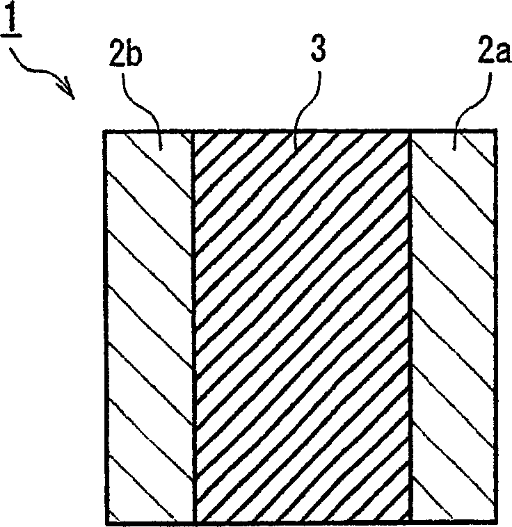
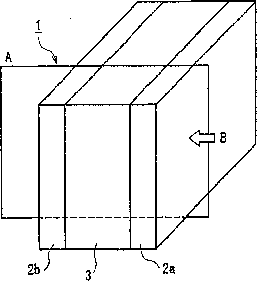
[0168] In Example 1, SrTiO was used as the transformation body 3 , produced as Figure 19 The thermal switching element 1 shown. Al is used for electrode 2a and electrode 2b, and Al is used for insulator 9 2 o 3 , Au is used for electrode 10. The manufacturing method of the thermal switch element 1 used in embodiment 1 is as follows Figures 20A-20E shown.
[0169] Initially, in SrTiO as transformation 3 3 Resist 20 ( Figure 20A ). As for the resist, a positive resist material is used, and a general resist coating method is used. Next, an Al layer 21 is deposited on the whole by sputtering ( Figure 20B ). Next, by lift-off, the resist 20 and the portion on the resist 20 in the Al layer 21 are removed to form the electrode 2a and the electrode 2b ( Figure 20C ). Next, the sputtering method is used to form Al 2 o 3 The insulator 9( Figure 20D ). Finally, an electrode 10 made of Au was formed by sputtering ( Figure 20E ),production Figure 19 The thermal sw...
Embodiment 2
[0177] In Example 2, SrTiO doped with Cr in the range of 0.1 atomic % to 10 atomic % was used as the transformation body 3 3 (Cr:SrTiO 3 ),production Figure 22 The thermal switching element 1 shown.
[0178] Initially, using SrTiO 3 As the substrate 22, SrRuO is formed on the substrate 22 by sputtering 3 constituted electrode 2a. Secondly, on the electrode 2a is formed by Cr:SiTiO 3 The formed transition body 3 was further formed with an electrode 2b made of Pt. The sputtering method is also used in forming the transition body 3 and the electrode 2b. The transformation body 3 and the electrode 2a are formed in a heating atmosphere at about 450°C to 700°C. Wherein, the thicknesses of the electrode 2a, the transition body 3 and the electrode 2b are about 200 nm, 300 nm and 2 μm, respectively.
[0179] For the thermal switching element 1 produced in this way, by applying a voltage between the electrodes 2a and 2b and applying electric energy to the transition body 3, cha...
Embodiment 3
[0183] In Example 3, SrTiO was used as Transformation 3 3 and LaSrMnO 3 laminated body made of Figure 23 The thermal switching element 1 shown.
[0184] Using Nb:SrTiO 3 As the base 22, the thin films shown below were deposited by laser ablation. The deposition is performed under an oxygen atmosphere of 10 mmTorr to 500 mmTorr while heating at 450°C to 700°C. Initially, SrTiO is configured on the substrate 22 3 (thickness 50nm), further configure LaSrMnO on it 3 (Thickness: 100 nm) as Transformer 3. Second, configure SrRuO on the transition body 3 3 (thickness 10nm). Next, the SrRuO 3 Pt (thickness 240nm) is arranged on it. The temperature during sputtering was 400°C. Next, if Figure 23 As shown for SrRuO 3 The laminated body of Pt and Pt is microfabricated to form electrode 2a and electrode 2b. Thereafter, as the insulator 9, Al was arranged so that the thickness from the surface of the electrode 2a and the electrode 2b was 80 nm. 2 o 3 , and finally, Au (th...
PUM
| Property | Measurement | Unit |
|---|---|---|
| Thickness | aaaaa | aaaaa |
| Thickness | aaaaa | aaaaa |
| Thickness | aaaaa | aaaaa |
Abstract
Description
Claims
Application Information
 - R&D
- Intellectual Property
- Life Sciences
- Materials
- Tech Scout
- Unparalleled Data Quality
- Higher Quality Content
- 60% Fewer Hallucinations
Browse by: Latest US Patents, China's latest patents, Technical Efficacy Thesaurus, Application Domain, Technology Topic, Popular Technical Reports.
© 2025 PatSnap. All rights reserved.Legal|Privacy policy|Modern Slavery Act Transparency Statement|Sitemap|About US| Contact US: help@patsnap.com