Semiconductor device having tin-based solder layer and method for manufacturing the same

A solder layer, semiconductor technology, applied in the direction of semiconductor/solid-state device manufacturing, semiconductor devices, semiconductor/solid-state device components, etc., can solve the problem of high manufacturing cost

Active Publication Date: 2006-03-15
DENSO CORP
View PDF1 Cites 15 Cited by
  • Summary
  • Abstract
  • Description
  • Claims
  • Application Information

AI Technical Summary

Problems solved by technology

Therefore, the manufacturing cost becomes higher

Method used


Image

  • Semiconductor device having tin-based solder layer and method for manufacturing the same
  • Semiconductor device having tin-based solder layer and method for manufacturing the same
  • Semiconductor device having tin-based solder layer and method for manufacturing the same

Examples


no. 1 example

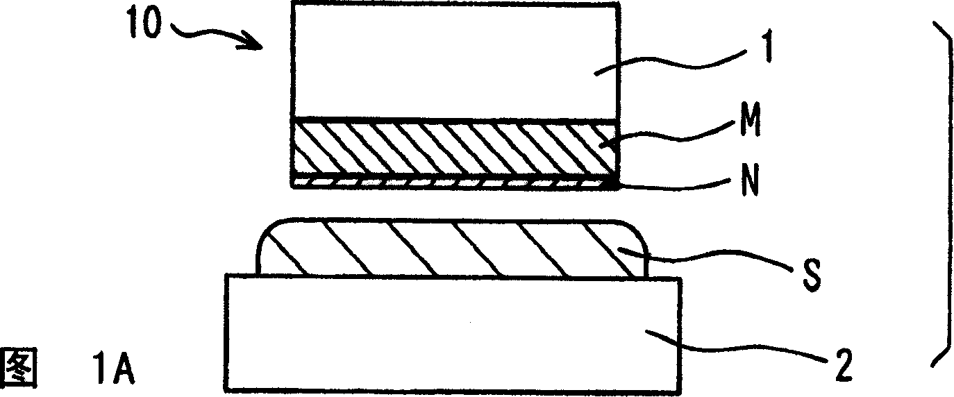
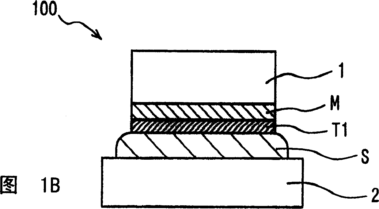
[0025] A semiconductor device 100 according to a first embodiment of the present invention is shown in 1A and 1B. FIG. 1A shows the device 100 before heat treatment, ie before soldering, and FIG. 1B shows the device 100 after heat treatment, ie after soldering.

[0026] The device 100 includes a semiconductor substrate 1 and a base member 2 . The substrate 1 has electronic components, such as power transistors, formed on the front side of the substrate 1 . The backside of the substrate 1 opposite the semiconductor component is bonded to the base component 2 with a layer S of tin-based solder. The base member 2 is, for example, a heat sink, a lead frame, or a circuit board. Device 100 was fabricated as follows.

[0027] First, electronic components are formed on the front side of the substrate 1 . A first metal layer M and a second metal layer N are sequentially formed on the backside of the substrate 1 . Thus, the semiconductor chip 10 is formed. Then, the chip 10 is mou...

no. 2 example

[0044] A semiconductor device 101 according to a second embodiment of the present invention is shown in Figure 6A to 6C. Figure 6A shows the chip 10 prior to the first heat treatment, Figure 6B The chip 10 after the first heat treatment and the base member 2 before soldering are shown. Figure 6C shows the device 101 after the second heat treatment, ie after soldering.

[0045] Device 101 was fabricated as follows. First, a first metal layer M and a second metal layer N are sequentially formed on the backside of the substrate 1 to prepare the semiconductor chip 10 . Chip 10 is first heated to form intermediate alloy layer O. The intermediate alloy layer O consists of a first metal and a second metal alloy. An intermediate alloy layer O is disposed between the first and second metal layers M, N. After this first heat treatment, the chip 10 is mounted on the base member 2 via the solder layer S. As shown in FIG. Then, the chip 10 and the base member 2 are heated a secon...


PUM

PropertyMeasurementUnit
thicknessaaaaaaaaaa
thicknessaaaaaaaaaa
thicknessaaaaaaaaaa

Abstract

A semiconductor device includes: a semiconductor substrate; a base member; a tin-based solder layer; a first metal layer; and a first alloy layer. The semiconductor substrate is bonded to the base member through the first metal layer, the first alloy layer and the tin-based solder layer in this order. The first alloy layer is made of a first metal in the first metal layer and tin in the tin-based solder layer. The first metal layer is made of at least one of material selected from the group consisting of titanium, aluminum, iron, molybdenum, chromium, vanadium and iron-nickel-chromium alloy.

Description

technical field [0001] The invention relates to a semiconductor device with a tin-based solder layer and a manufacturing method thereof. Background technique [0002] Conventionally, lead-tin alloy (Pb-Sn alloy) solder is used to bond semiconductor substrates such as IC chips having semiconductor devices to base members such as heat sinks and lead frames. However, in consideration of environmental protection such as safety and low damage, it is required to use Pb-free solder or low-Pb-containing solder. One of the Pb-free solders is tin-based solder. [0003] Japanese Patent Application Laid-Open No. 2003-347487 discloses bonding the backside of a semiconductor substrate to a base member with tin-based solder. The substrate includes a backside electrode. The electrodes consist of layers of titanium, nickel, and gold or silver, which are stacked sequentially on a substrate. The base member is a heat radiation member. The substrate is mounted on the heat radiation member ...

Claims


Application Information

Patent Timeline
Patent Type & Authority Applications(China)
IPC IPC(8): H01L23/48H01L23/12H01L25/00H01L21/60H05K1/18H05K3/34
CPCH01L2924/014H01L23/4827H01L2924/01023H01L2224/04026H01L24/05H01L2924/01042H01L2924/01024H01L2924/01013
Inventor 粥川君治棚桥昭则武千景三浦昭二
Owner DENSO CORP
Why Eureka
Try Eureka