
Configuration system of chip identifying code and con figuration method

A chip identification and configuration system technology, applied in electrical components, electrical solid devices, circuits, etc., can solve problems such as increasing chip design and manufacturing costs, and achieve the effect of reducing chip R&D and manufacturing costs and small changes to silicon chips

Inactive Publication Date: 2006-05-24
VIMICRO CORP
View PDF0 Cites 0 Cited by
  • Summary
  • Abstract
  • Description
  • Claims
  • Application Information

AI Technical Summary

Problems solved by technology

In this case, if the metal layer corresponding to the Chip ID configuration circuit is not in the n metal layers, for example, the second and third metal layers need to be modified, and the Chip ID is in the first metal layer, then according to the above Chip ID In the configuration mode, a total of 3 metal layers need to be changed, that is, n+1 metal layers need to be modified, thus greatly increasing the cost of chip design and manufacturing

Method used


Image

  • Configuration system of chip identifying code and con figuration method
  • Configuration system of chip identifying code and con figuration method
  • Configuration system of chip identifying code and con figuration method

Examples


Embodiment Construction

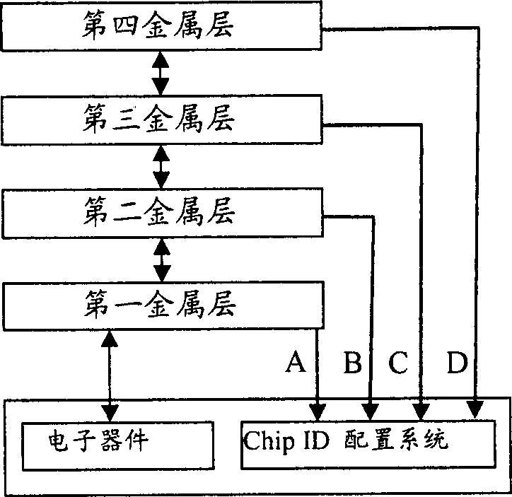
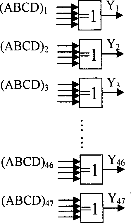
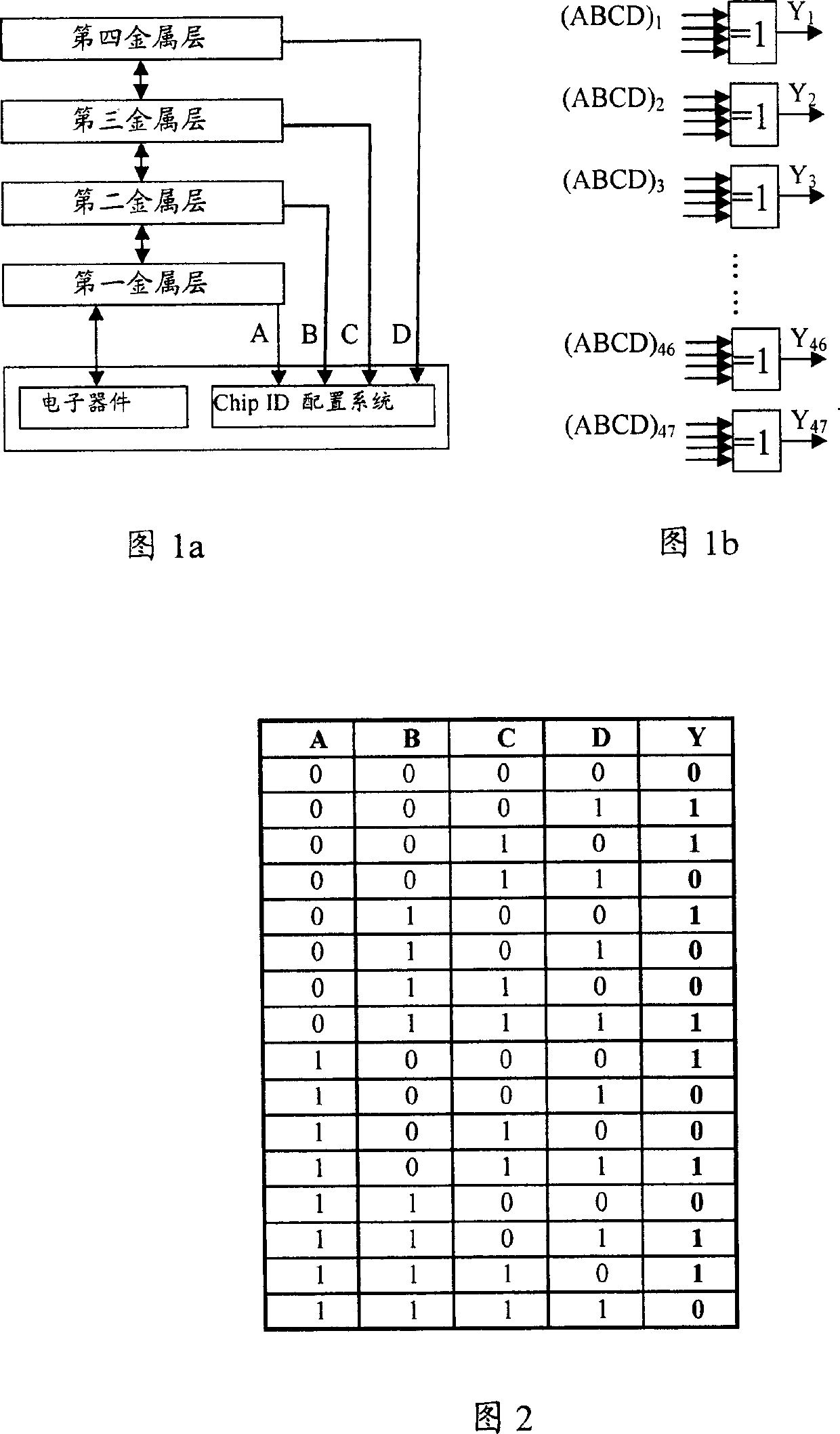
[0030] The core content of the Chip ID configuration system, configuration method and modification method of the present invention is to utilize the characteristics of a multi-input XOR gate, that is, changing any logic value in its input will cause the output logic value of the XOR gate to occur. Change.

[0031] The Chip ID configuration system and configuration method of the present invention will be further described with a specific embodiment below in conjunction with the accompanying drawings.

[0032] In the chip, the Chip ID is represented by binary data. If people need to read it, the read value can be hexadecimal data, or it can be further expressed as an ASCII string. In order to facilitate identification, in the following description, if necessary, an ASCII character string is used to represent the Chip ID.

[0033] In this example, assume that the chip has four metal layers, and the ASCII code value of the chip has the chip identification code "CHIP21".

[0034]...


PUM


Abstract

The system includes some exclusive-or gates. Number of input end of each exclusive-or gate is equal to number of metal layers. Each input end of each exclusive-or gate is corresponding to each metal layer, and then each input end is connected to electrical source or ground of corresponding metal layer. An output of each exclusive-or gate represents one bit of binary number. All outputs from exclusive-or gates constitute string in binary to represent ID code of chip. The invention also discloses method for configuring ID code of chip. Advantages are: changing ID code of chip by minimal change made for chip, and lowering cost. The invention is suitable to chip in structure of multiple metal layers, and applicable to procedure for designing and manufacturing IC.

Description

technical field [0001] The invention relates to the field of integrated circuits, in particular to a chip identification code configuration system, configuration method and modification method. Background technique [0002] In the process of designing and manufacturing integrated circuit chips, chip design engineers need to use the chip identification code, that is, Chip ID to record the design / manufacturing records of the chip, and software engineers (including driver or firmware engineers) also need a unique Chip ID to Identify chips of different batches or functions. [0003] In order to better understand the configuration of the chip ID, here is a brief introduction to the manufacture of the chip. The manufacture of chips can be divided into two main parts, one is to manufacture active and passive devices on the surface of the wafer, and the other is to use metal systems to connect various devices. [0004] In the era of medium-scale integrated circuits, only a single-...

Claims


Application Information

Patent Timeline
Patent Type & Authority Applications(China)
IPC IPC(8): H01L23/544
Inventor 温小勇朱军
Owner VIMICRO CORP
Learn More