Device for debugging circuit board, and method for debugging circuit board

A technology for circuit boards and integrated circuits is applied in the field of circuit board debugging devices, which can solve problems such as inability to implement and difficult to operate, and achieve the effects of reducing costs, avoiding damage, and improving debugging effects.

Inactive Publication Date: 2006-07-05
NAT SPACE SCI CENT CAS
View PDF0 Cites 11 Cited by
  • Summary
  • Abstract
  • Description
  • Claims
  • Application Information

AI Technical Summary

Problems solved by technology

Secondly, whether it is secant line or flying line operation, it is very difficult to operate the densely distributed and narrowly spaced circuit traces on the printed circuit board, and it is very easy to cause undesired short circuits and open circuits that are difficult to find. It brings side effects that cannot be ignored; mo...

Method used


Image

  • Device for debugging circuit board, and method for debugging circuit board
  • Device for debugging circuit board, and method for debugging circuit board

Examples


Embodiment Construction

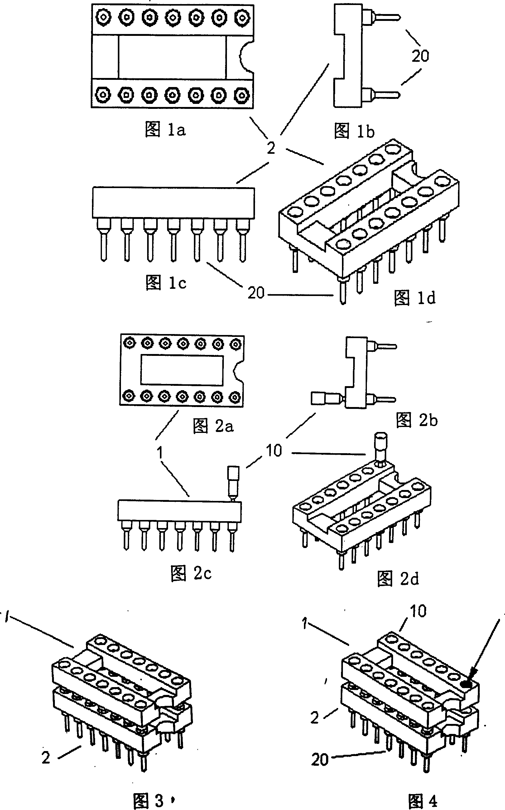
[0031] The present invention is described in detail below in conjunction with accompanying drawing and embodiment: with reference to Fig. The pin socket 2 and the movable pin socket 1 are general dual-in-line sockets purchased on the market. There are removable movable pins 10 in the jack of the movable pin socket 1, and the fixed pin socket 2 is located The bottom layer of the device has metal fixed pins 20, which are welded to the printed circuit board; the movable pin socket 1 is plugged into the fixed pin socket 2, and the jacks on the pins are used for the integration of the dual in-line package Circuit chip insertion.

[0032] The circuit board debugging device mentioned in the present invention is based on a common dual in-line package chip socket. There are two methods for making the movable pin socket mentioned in the present invention:

[0033] (1) Adopt ordinary dual-in-line package chip socket, but the pins on the socket are fixed and cannot be moved, so just pul...


PUM


Abstract

The invention discloses a circuit board debugging device and method, comprising a fixed needle socket and an active needle socket, where the fixed pin socket is in the bottom layer and welded to a printed circuit board (PCB), and the active needle socket is plugged in the fixed needle socket and provided with extractable needles, and the jacks on the extractable needles are used for DIP integrated circuit (IC) chips to be inserted in. As measuring, the pins of the extractable needles are suspended and do no contact with the fixed needle socket so that the circuit is cut-off; therefore the invention has no destruction to IC chips and PCBs, thus improving the circuit board debugging effect. And it can accurately locate failures and besides, the suspended pins are easy for fixing the probes of oscillographs and logic analyzers, beneficial to measurement.

Description

technical field [0001] The invention relates to a circuit board debugging device, in particular to a circuit board debugging device using dual in-line packaged chips and a circuit board debugging method. Background technique [0002] At present, there are many circuit boards in various electronic equipment and devices to complete various functions and tasks, and various integrated circuit chips play a decisive role on the circuit boards. Integrated circuit chips come in a variety of packages, such as dual in-line package (DIP), plastic quad flat package (PQFP), pin grid array package (PGA), ball grid array package (BGA), etc. . Among them, the vast majority of small and medium-sized integrated circuits (ICs) are in the form of dual in-line packages (DIP), such as 8088, RAM, FIFO and other devices in Intel series CPUs. [0003] When debugging the entire circuit board, the circuit traces and component pins on the circuit board can be measured and analyzed by an oscilloscope ...

Claims


Application Information

Patent Timeline
IPC IPC(8): G01R1/02G01R31/00
Inventor 曹松陈斌沈卫华陈小敏孙辉先
Owner NAT SPACE SCI CENT CAS
Why Eureka
Try Eureka