Optical information medium
A technology of optical information and media, applied in the field of optical information media, can solve problems such as insufficient storage capacity and the impact of errors
- Summary
- Abstract
- Description
- Claims
- Application Information
AI Technical Summary
Problems solved by technology
Method used
Image
Examples
Embodiment 1
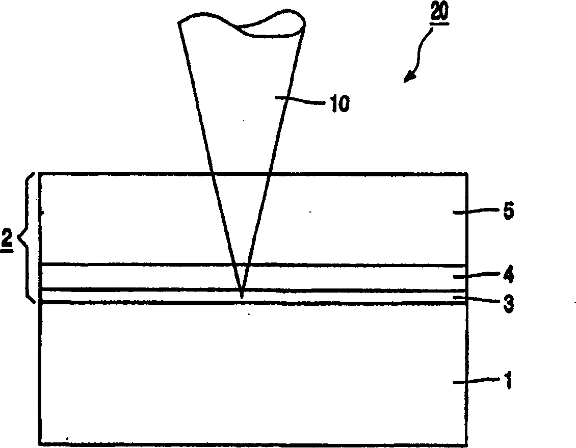
[0035] in the attached figure 1 A first exemplary embodiment of an erasably recordable optical information medium 20 according to the DVR-Blue format is shown in . A radiation beam 10 having a radiation wavelength λ of 405 nm and a numerical aperture NA of 0.85 is focused in a medium 20 . The medium 20 has a substrate 1 and a stack 2 of layers provided thereon. Stack 2 includes a first recording stack 3 with an IPIM layer structure, in this order, where I is composed of (ZnS) 80 (SiO 2 ) 20 Fabricated dielectric layer, P is a compound with Ge 14 Sb 28 Te 5 8 phase change alloy, M is the metal mirror layer of aluminum (Al). The thicknesses of the layers in IPIM recording stack 3 are 115 nm, 27 nm, 26 nm and 100 nm, respectively. The Al layer is in the vicinity of the substrate 1 . The stack 2 further comprises two radiation beam transmissive layers 4 , 5 . The first transmission layer 4 is made of ultraviolet curing resin, such as Daicure EX-860 provided by Dainippon...
Embodiment 2
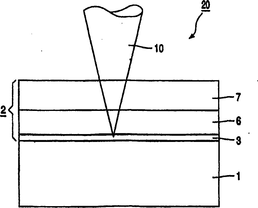
[0039] in the attached figure 2 A second exemplary embodiment of an erasably recordable optical information medium 20 according to the DVR-Blue format is shown in . A radiation beam 10 having a radiation wavelength λ of 405 nm and a numerical aperture NA of 0.85 is focused in a medium 20 . The medium 20 has a substrate 1 and a stack 2 of layers provided thereon. The stack 2 comprises a first recording stack 3 identical to the stack 3 described in exemplary embodiment 1 and two radiation beam transmissive layers 6 , 7 . The first transmissive layer 6 is made of a layer of pressure sensitive adhesive (PSA) commercially available from eg 3M. The PSA layer 6 may comprise a transparent backing and / or a carrier layer, such as an optionally surface-treated amorphous polymer layer, such as polyethylene terephthalate (PET) with an adhesive layer on each side. , PC or polymethyl methacrylate (PMMA) layer, but preferably it is a transfer film that does not include a backing and / or ca...
Embodiment 3
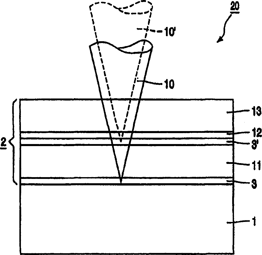
[0043] in the attached image 3 A third exemplary embodiment of an erasably recordable optical information medium 20 according to the DVR-Blue format but with an additional second recording layer is shown in . A radiation beam 10 having a radiation wavelength λ of 405 nm and a numerical aperture NA of 0.85 is focused in a medium 20 . The medium 20 has a substrate 1 and a stack 2 of layers provided thereon. The stack 2 comprises a first recording stack 3 , a second recording stack 3 ′ and three radiation beam transmissive layers 11 , 12 , 13 . The first recording stack 3 has an IPIM structure similar to that of the exemplary embodiment 1, including in the following order:
[0044] - Dielectric layer (ZnS) with a thickness of 30 nm 80 (SiO 2 ) 20 ,
[0045] - Compound GeSb with a thickness of 25 nm 2 Te 4 record layer,
[0046] - Dielectric layer (ZnS) with a thickness of 15 nm 80 (SiO 2 ) 20 ,
[0047] - An aluminum mirror layer adjacent to the substrate with a thi...
PUM
| Property | Measurement | Unit |
|---|---|---|
| thickness | aaaaa | aaaaa |
| thickness | aaaaa | aaaaa |
| thickness | aaaaa | aaaaa |
Abstract
Description
Claims
Application Information


