Universal probe device for electronic module detecting system

A technology of electronic components and probes, applied in the field of probe devices for panel array testing, can solve the problems of probe frame production and design costs, production capacity and manpower waste, time-consuming, etc., and achieve simple and fast design and manufacture, and fast replacement steps , Low cost effect

Active Publication Date: 2006-08-23
AU OPTRONICS CORP
View PDF0 Cites 16 Cited by
  • Summary
  • Abstract
  • Description
  • Claims
  • Application Information

AI Technical Summary

Problems solved by technology

Because a frame with a specific specification is usually not suitable for other products, this will cause additional costs for the production and design of the probe frame, and the production and delivery of the probe frame will take a long time
In addition, when changing the product line for testing, the steps of changing the probe frame are also quite time-consuming, resulting in a waste of production capacity and manpower for various reasons

Method used


Image

  • Universal probe device for electronic module detecting system
  • Universal probe device for electronic module detecting system
  • Universal probe device for electronic module detecting system

Examples


Embodiment Construction

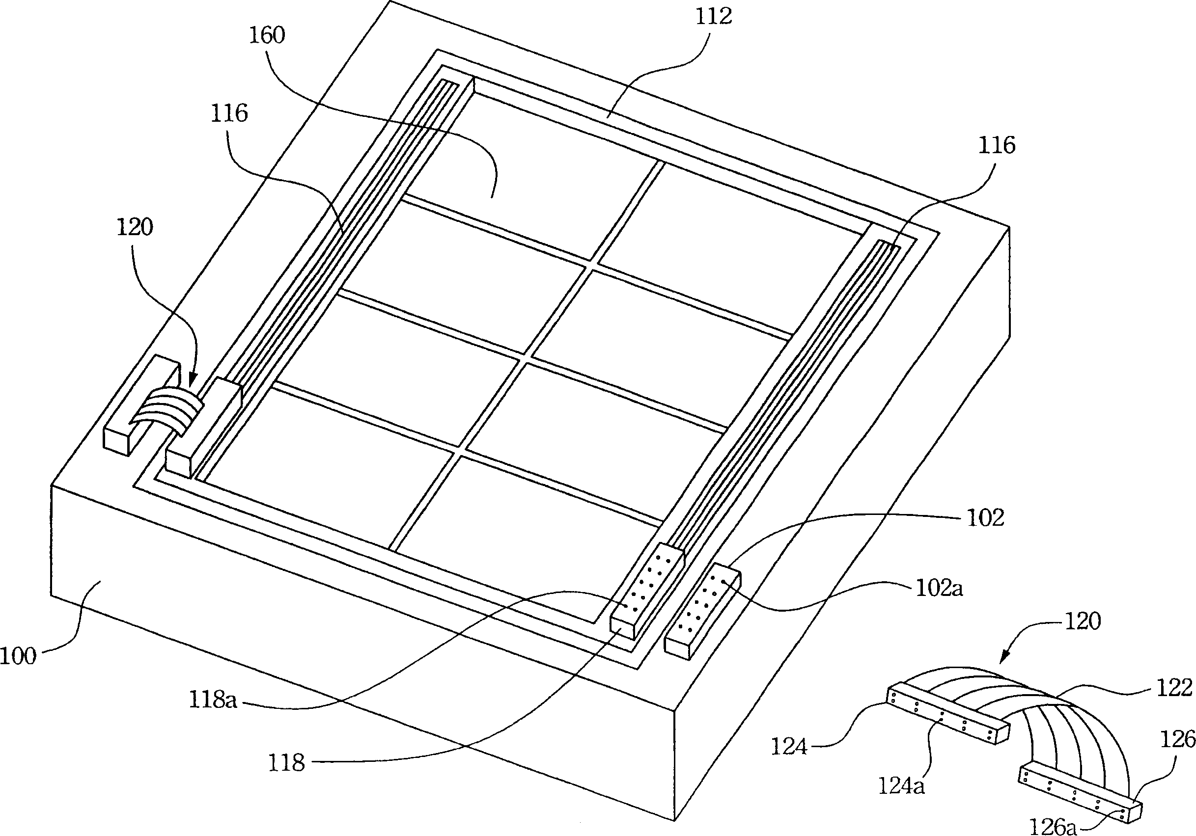
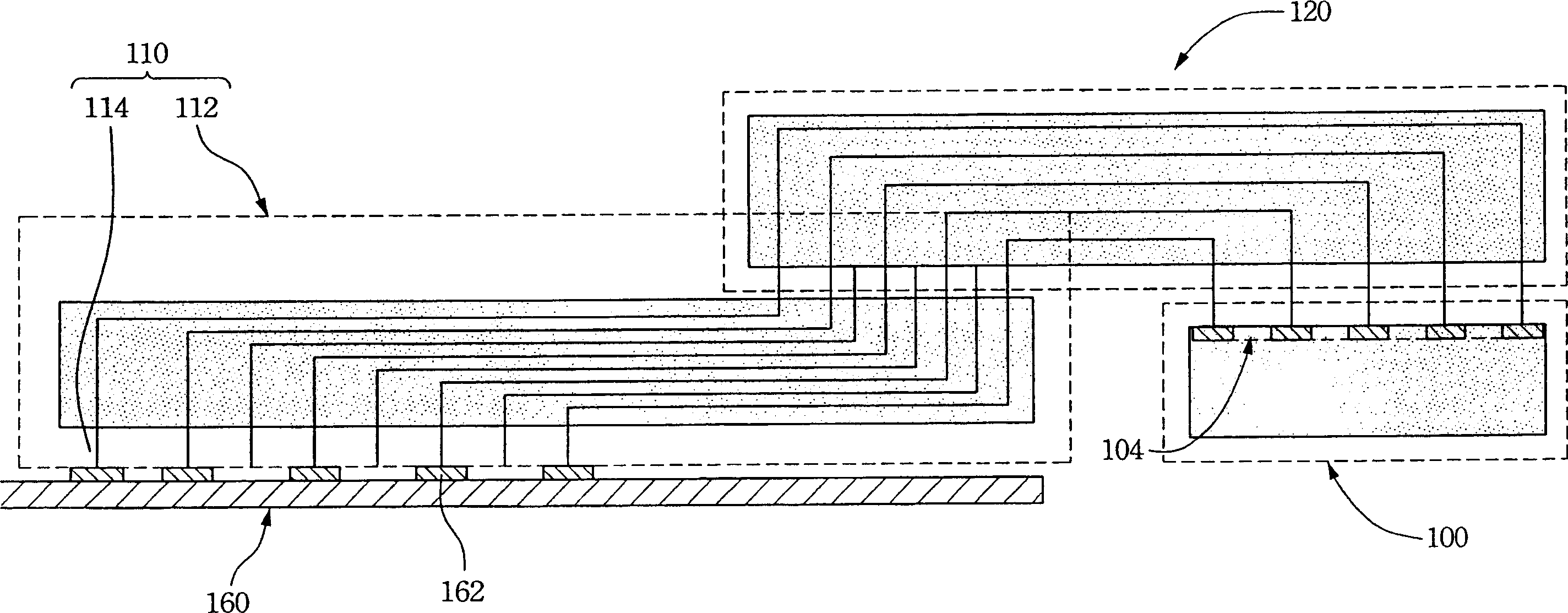
[0036] The present invention discloses a probe device for system testing of electronic components. A shared probe unit is provided to perform test steps for display panels of different sizes and specifications. When changing a product line for testing, only a circuit switching device needs to be replaced, which avoids the traditional need for additional design. , the inconvenience of making and replacing the probe frame and a large amount of cost. In order to make the narration of the present invention more detailed and complete, refer to the following description and cooperate Figure 1a and Figure 1b icon.

[0037] refer to Figure 1a , which shows a schematic diagram of a preferred embodiment of a probe device for system testing of electronic components according to the present invention. The probe device of the electronic component system test of the present invention includes a probe unit 110 (shown in Figure 1b ) and a line switching device 120. The probe unit 110 i...


PUM


Abstract

This invention relates to a universal probe device used in an electronic component test system including a probe unit and a circuit switch device, in which, the probe unit includes a bracket base and multiple probes set on the base to test the electronic component system, the circuit switch device is used in electrically connecting probes corresponding to different panels with the test signal source.

Description

technical field [0001] The present invention relates to a probe device for system testing of electronic components, and in particular to a probe device for panel array testing. Background technique [0002] Applications of flat panel displays are expanding rapidly as they extend to word processors, desktop personal computers, handheld television displays, and similar applications. In particular, liquid crystal display (Liquid Crystal Display: LCD) panels are widely used in various applications due to their mature manufacturing technology. With the advancement of manufacturing technology, the size of the display panel has also developed a variety of specifications to meet different usage needs, because the LCD panel is composed of many liquid crystal packages and other components. In addition, the larger LCD panel has more s component. Even if only one component in the LCD panel fails, the entire LCD panel fails. Therefore, before the liquid crystal display panel is packag...

Claims


Application Information

Patent Timeline
Patent Type & Authority Applications(China)
IPC IPC(8): G01R1/073G01R31/00G09G3/00G01M11/00G02F1/13
Inventor 张钦亮
Owner AU OPTRONICS CORP
Why Eureka
Try Eureka