Supercharge Your Innovation With Domain-Expert AI Agents!

Piezo-oscillator

A technology of piezoelectric oscillators and piezoelectric elements, applied in power oscillators, electric solid-state devices, circuits, etc., to achieve the effect of improving instability

Inactive Publication Date: 2006-08-23
SEIKO EPSON CORP +1
View PDF1 Cites 3 Cited by
  • Summary
  • Abstract
  • Description
  • Claims
  • Application Information

AI Technical Summary

Problems solved by technology

[0012] On the other hand, since the generation of hot carriers involves the increase and decrease of holes in the inversion layer 110, it takes a certain time

Method used


Image

  • Piezo-oscillator
  • Piezo-oscillator
  • Piezo-oscillator

Examples


Embodiment Construction

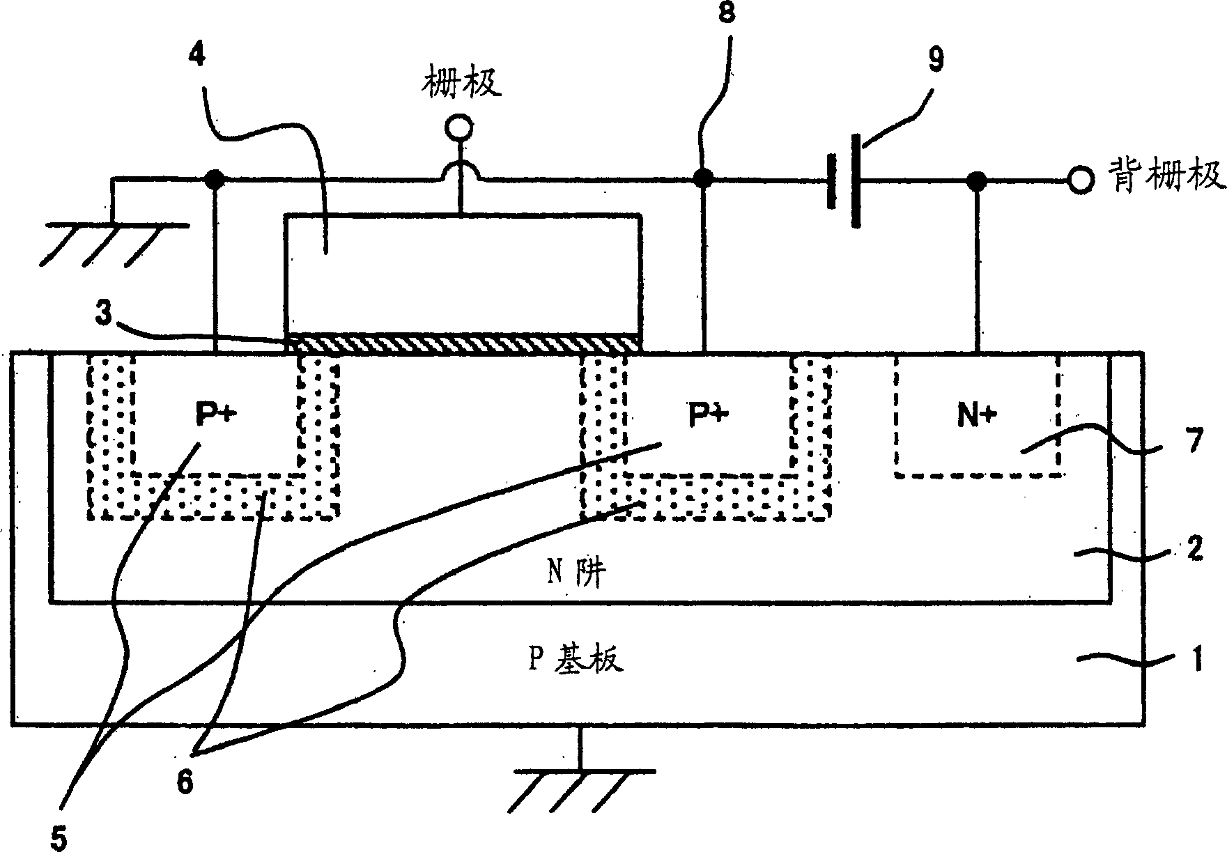
[0054] figure 1 It is a structural diagram of a P-channel (Pch) transistor type MOS capacitive element provided in an IC used in the present invention. exist Figures 1 to 9 Among them, the first conductivity type is N type and the second conductivity type is P type.

[0055] exist figure 1 , the silicon substrate (P-sub) 1 of the second conductivity type (P-type) is grounded. A well region (hereinafter referred to as an N well layer) 2 of a first conductivity type opposite to a second conductivity type is formed on the P-sub1. Gate oxide film layer 3 including silicon oxide serving as an insulator is formed on N well layer 2 . A gate layer 4 including polysilicon is formed on the gate oxide film layer 3 . The gate is drawn out from the gate layer 4 as an external terminal. A lead-out electrode 5 of a second conductivity type (P-type) with a high acceptor impurity concentration is formed on the N well layer 2 at two positions close to the gate oxide film layer 3 (the d...


PUM


Abstract

Deterioration in frequency stability with time in a conventional piezoelectric oscillator using an accumulation type MOS capacitance element is improved. A P-channel transistor type or an N-channel transistor type is used as a MOS capacitance element in a variable capacitance circuit used in a piezoelectric oscillator. A bias voltage is applied between P-type or N-type extraction electrodes formed in source and drain regions and an N-type extraction electrode provided in an N-well region or a P-type extraction electrode provided in a P-well region. Instability in the MOS capacitance element with time is thus eliminated.

Description

technical field [0001] The present invention relates to a piezoelectric oscillator, and more particularly, to a piezoelectric oscillator using a variable capacitance circuit using a MOS capacitance element for frequency voltage control, frequency temperature compensation, and the like. Background technique [0002] As a variable capacitance element replacing a variable capacitance diode, a MOS capacitance element is attracting attention at present. In applications such as temperature-compensated crystal resonators (hereinafter referred to as TCXOs) such as cellular phones, MOS capacitive elements have a feature of obtaining large capacitance changes even with slight voltage changes. Therefore, even in a case where the voltage applicable to the variable capacitance element must be set low because the voltage for the oscillation circuit becomes low, the MOS capacitance element has sufficient capacitance characteristics for practical use. [0003] Figure 12 The structure of a...

Claims


Application Information

Patent Timeline
Patent Type & Authority Applications(China)
IPC IPC(8): H03B5/32H03B5/36H01L27/04H01L27/08H03B5/04
CPCH03B5/366H01L27/0808H01L27/0811H03B5/04H03B5/32H03B5/36
Inventor 大岛刚黑后重久石川匡亨黑泽晋藤本裕希中柴康隆
Owner SEIKO EPSON CORP
Features
  • R&D
  • Intellectual Property
  • Life Sciences
  • Materials
  • Tech Scout
  • Unparalleled Data Quality
  • Higher Quality Content
  • 60% Fewer Hallucinations
Learn More