Non-volatile memory possessing a plurality of capture film

A technology of non-volatile storage and devices, applied in the field of non-volatile storage devices and manufacturing such devices, can solve the problems of improving programming and erasing efficiency while improving difficulties

Inactive Publication Date: 2006-09-13
SAMSUNG ELECTRONICS CO LTD
View PDF1 Cites 23 Cited by
  • Summary
  • Abstract
  • Description
  • Claims
  • Application Information

AI Technical Summary

Problems solved by technology

Therefore, for including figure 1 It is difficult to improve programming and erasing efficiencies while improving or maintaining retention characteristics for semiconductor devices whose structure corresponds substantially to that of the illustrated device

Method used


Image

  • Non-volatile memory possessing a plurality of capture film
  • Non-volatile memory possessing a plurality of capture film
  • Non-volatile memory possessing a plurality of capture film

Examples


Embodiment Construction

[0026] The present invention will now be described more fully with reference to the accompanying drawings, in which certain exemplary embodiments of the invention are shown. Those skilled in the art will appreciate, however, that the present invention may be embodied in many different forms and should not be construed as limited to the embodiments set forth herein. Rather, these embodiments are provided so that this disclosure will be thorough and complete, and will fully convey the concept of the invention to those skilled in the art.

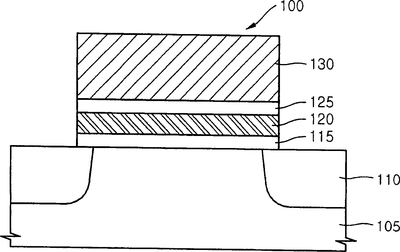
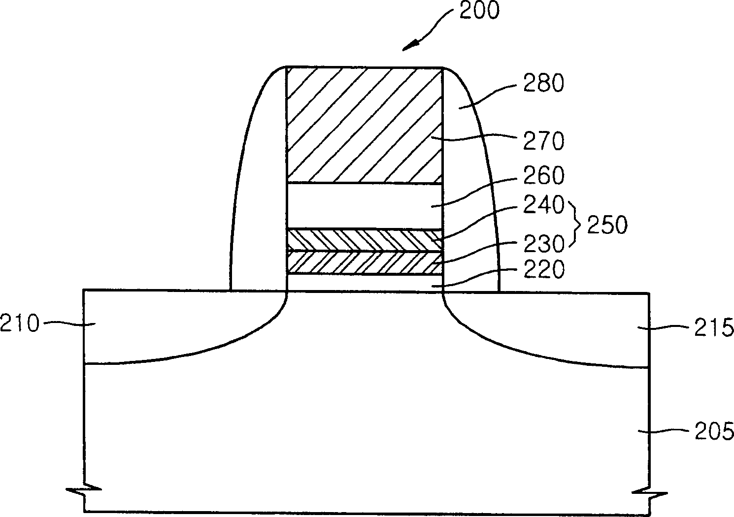
[0027] image 3 is a cross-sectional view illustrating a nonvolatile memory device 200 according to an exemplary embodiment of the present invention. Such as image 3 As shown, the nonvolatile memory device 200 according to this exemplary embodiment of the present invention includes a tunnel insulating film 220 formed between source and drain regions 210, 215 on a semiconductor substrate 205, a storage node 250, a blocking insulating film 260...


PUM


Abstract

The present invention provides one kind of non-volatile memory, which includes tunnel insulating film formed on the semiconductor substrate, memory nodes formed on the tunnel insulating film, barrier insulating film formed on the memory nodes, and control grid formed on the barrier insulating film. The memory node includes at least two layers of capture film of different trap density, and the barrier insulating film possesses dielectric constant greater than that of silicon oxide film.

Description

technical field [0001] The present invention relates to nonvolatile memory devices and methods of fabricating such devices, and more particularly, to nonvolatile memory devices including storage nodes for storing charge and methods of fabricating memory devices including such storage nodes. Background technique [0002] During writing and erasing data, non-volatile memory devices may utilize one or more methods including, for example, modifying the threshold voltage transitions of transistors, shifting charge, and / or changing resistance. Those non-volatile memory devices that utilize this method of modifying threshold voltage transitions typically include storage nodes for storing charge and thus may be referred to as charge storing memory devices. Examples of the electricity storage memory device include a floating gate memory device using a floating gate as a storage node and a SONOS memory device using a charge trapping layer as a storage node. [0003] figure 1 is a cr...

Claims


Application Information

Patent Timeline
Patent Type & Authority Applications(China)
IPC IPC(8): H01L29/792H01L27/115
CPCH01L29/4232H01L29/513H01L29/792H01L29/7881H01L29/42324
Inventor 金柱亨韩祯希金桢雨闵约赛金汶庆郑渊硕
Owner SAMSUNG ELECTRONICS CO LTD
Why Eureka
Try Eureka