Bistable multi-resonant circuit
A multivibrator, bistable technology, applied in static memory, instruments, electrical components, etc., can solve the problem of increasing the circuit scale, such as the transmission gate transistor 108
- Summary
- Abstract
- Description
- Claims
- Application Information
AI Technical Summary
Problems solved by technology
Method used
Image

Examples
Embodiment 1
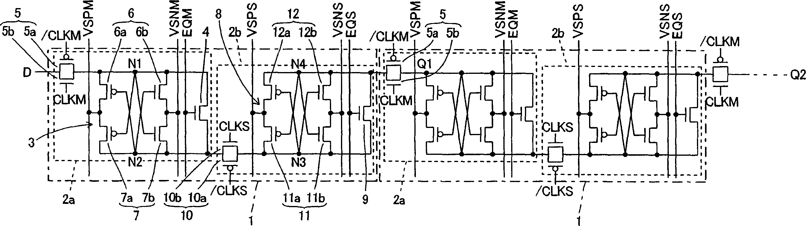
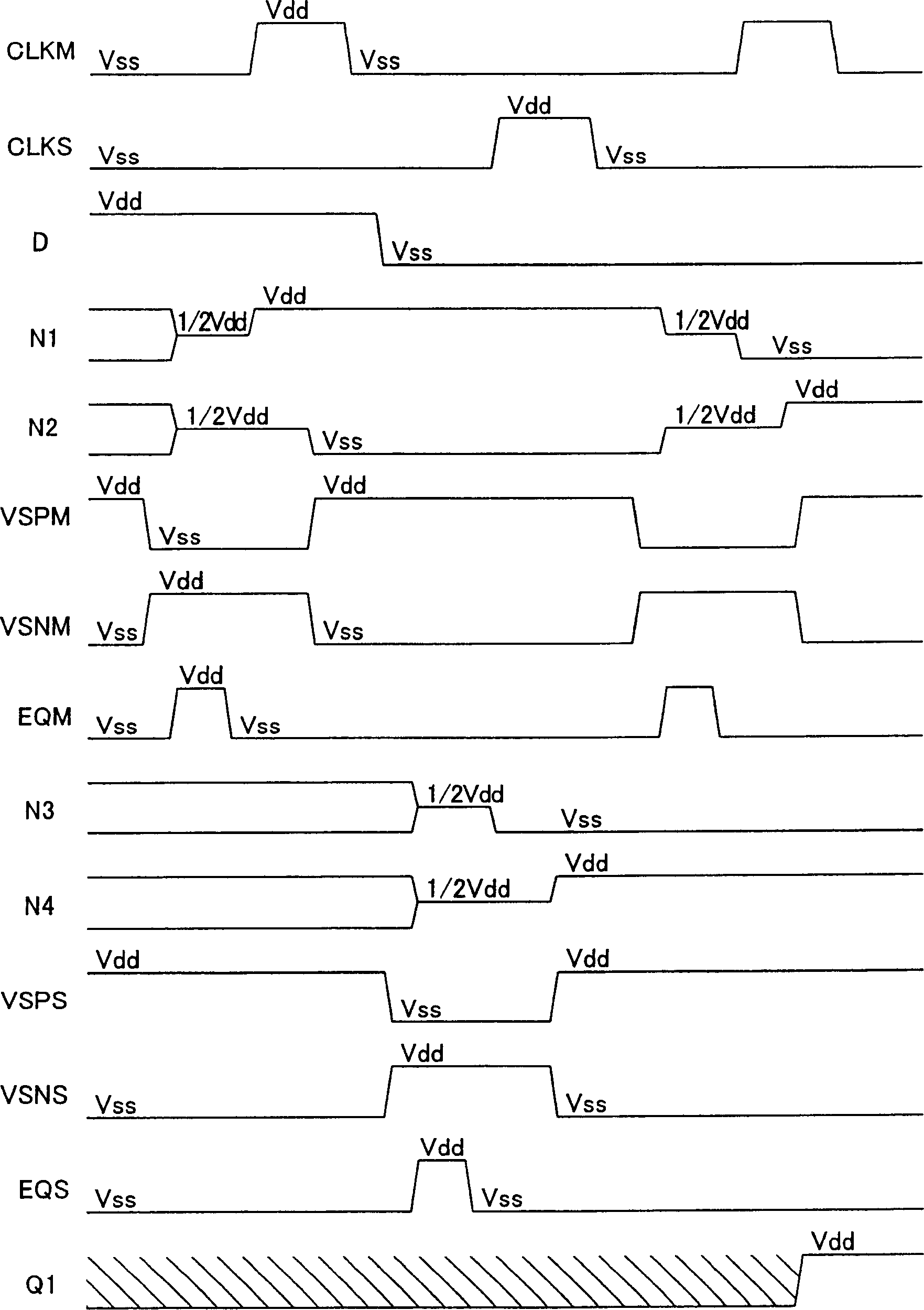
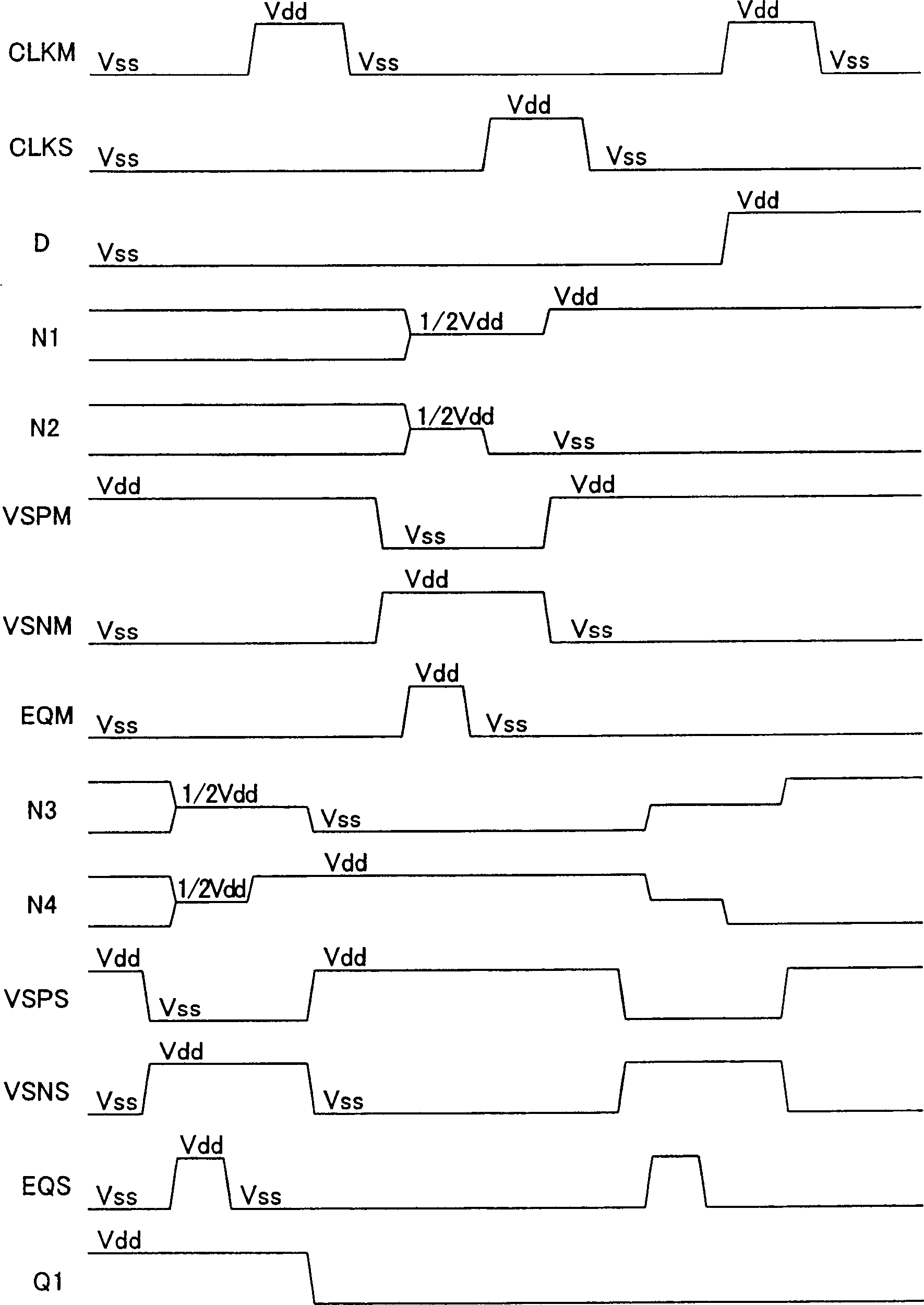
[0043] First, refer to figure 1 The circuit configuration of the shift register circuit using the flip-flop circuit according to the first embodiment will be described.
[0044] The shift register circuit of the embodiment 1 is as figure 1 As shown, it consists of a multi-stage bistable multivibrator circuit 1 connected in series. In addition, the multistage flip-flop circuit is constituted by two stages of delay latch circuits 2a and 2b, respectively. In addition, these delay latch circuits 2a and 2b are examples of the "first latch circuit" and the "second latch circuit" of the present invention, respectively. A given input signal is input from the node D to the delay gate circuit 2a of the first stage, and after the given input signal is locked for a certain period of time, an inverted phase of the given input signal is output to the delay gate circuit 2b of the second stage. Signal. In addition, the output signal from the delay gate circuit 2a of the first stage is i...
Embodiment 2
[0086] Refer below Figure 8 The structure of the DRAM using the shift register circuit including the flip-flop circuit according to the second embodiment will be described.
[0087] The DRAM of embodiment 2 such as Figure 8As shown, memory cell 21 provided at the intersection of word line WL and bit line BL1, shift register circuit 22, and n-channel transistors 23a and 23b are included. The memory cell 21 is composed of an n-channel transistor 21a and a capacitor 21b. In addition, the gate of n-channel transistor 21a is connected to word line WL. In addition, the capacitor 21 b holds charges corresponding to data stored in the memory unit 21 . In addition, the n-channel transistors 23 a and 23 b are respectively connected so that one of the source / drain regions is connected to the bit lines BL1 and BL2 , and the other is connected to the shift register circuit 22 .
[0088] The shift register circuit 22 is composed of a plurality of flip-flop circuits 31 connected in ser...
PUM
 Abstract
Description
Claims
Application Information
 - R&D
- Intellectual Property
- Life Sciences
- Materials
- Tech Scout
- Unparalleled Data Quality
- Higher Quality Content
- 60% Fewer Hallucinations
Browse by: Latest US Patents, China's latest patents, Technical Efficacy Thesaurus, Application Domain, Technology Topic, Popular Technical Reports.
© 2025 PatSnap. All rights reserved.Legal|Privacy policy|Modern Slavery Act Transparency Statement|Sitemap|About US| Contact US: help@patsnap.com