Semiconductor memory device operating with low current consumption

a memory device and semiconductor technology, applied in the direction of information storage, static storage, digital storage, etc., can solve the problems of noise, inability to be neglected, and required data read operation sense current of the order of 10 ma

Inactive Publication Date: 2004-02-12
RENESAS ELECTRONICS CORP
View PDF5 Cites 75 Cited by
  • Summary
  • Abstract
  • Description
  • Claims
  • Application Information

AI Technical Summary

Problems solved by technology

GMR element has a resistance changing rate ranging from 6 to 8%, and has a disadvantage that a sense current of the order of 10 mA is required in a data read operation.
Therefore, if characteristics of the access transistors vary, read current differ among the access transistors, and noises caused by these variations cannot be neglected.
Therefore, it is difficult to remove completely the offset in output voltage of the memory cell, which is caused by variations in characteristics of the access transistors.
Accordingly, if variation is present in film thickness of the tunnel film, this increases difference in resistance value of the tunneling film between the selected memory cell and the dummy cell, so that differential input voltages to the differential amplifier may become insufficient or inverted.
Therefore, the memory cell data cannot possibly be accurately detected.
Accordingly, the leakage currents in this drive circuit group increase the current consumption during the standby, so that a specification requirement of an ultra low standby current, which is required for application such as portable equipment, cannot be satisfied, and the application range is restricted.
In this case, however, the responsivility of the MOS transistor is deteriorated, and a drive current also decreases, if the transistor size is unchanged.
Accordingly, if the absolute value of the threshold voltage is made great, it is impossible to reduce the transistor sizes for a faster operation, and thus the device shrinking is impeded.
When the substrate bias is changed in accordance with the write and read cycles, a response delay may occur.

Method used


Image

  • Semiconductor memory device operating with low current consumption
  • Semiconductor memory device operating with low current consumption
  • Semiconductor memory device operating with low current consumption

Examples


Embodiment Construction

]

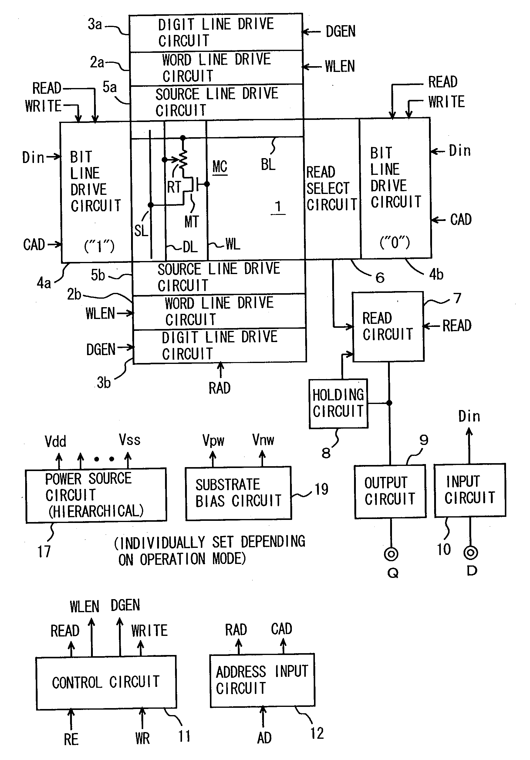
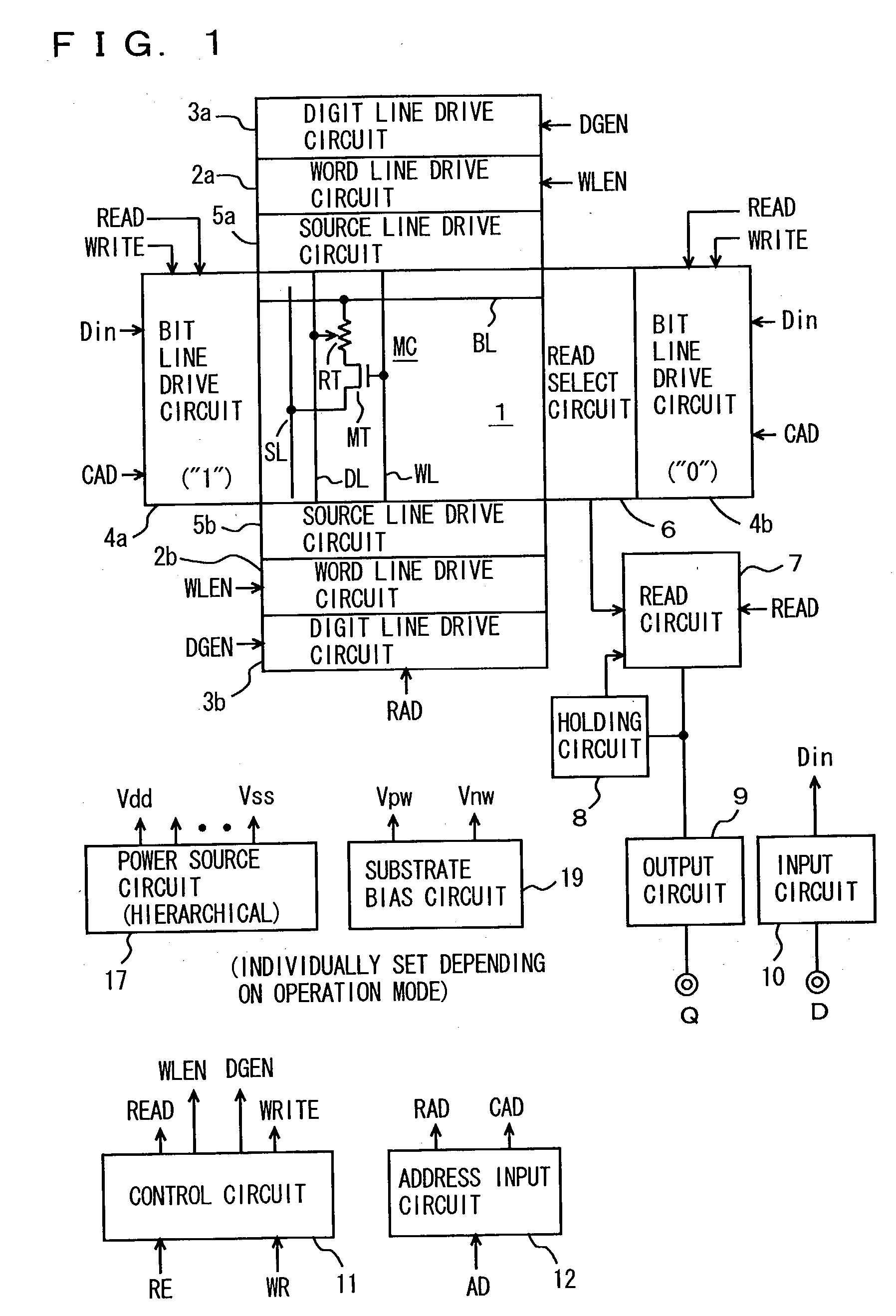
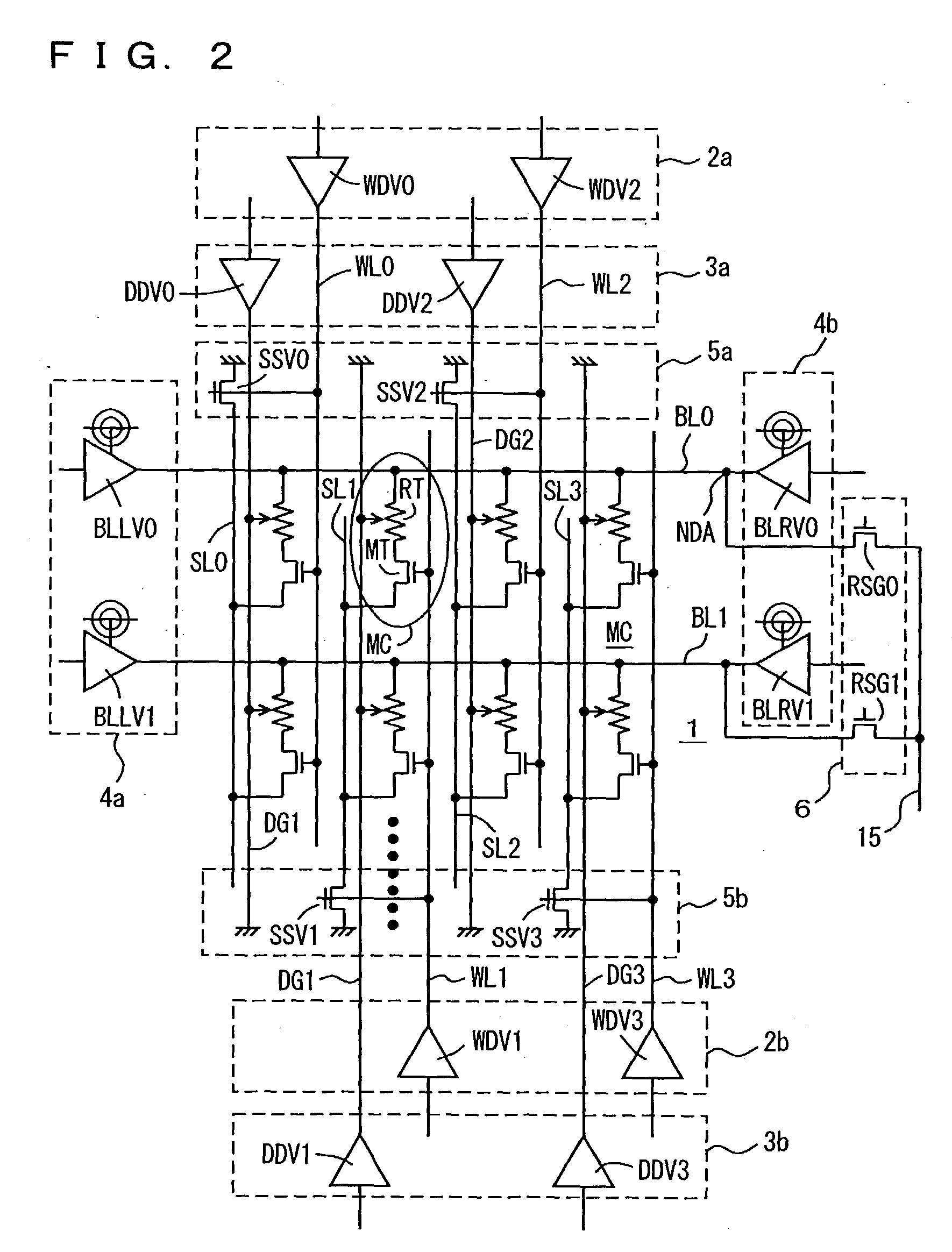
[0300] According to the foregoing description, in the memory cell data read operation, reference data is written, and then is compared with data read from the selected memory cell for determining the memory cell data. However, the constructions of the power supply and the substrate bias can be applied to the construction, in which a dummy cell is arranged in a memory cell array, and data of this dummy cell is compared with data from a selected memory cell.

[0301] The description has been given on the nonvolatile semiconductor memory device, in which induced magnetic fields cause polarization in the storage portion of the memory cell for nonvolatilely storing the data in accordance with the direction of polarization. However, the nonvolatile semiconductor memory device is not restricted to such MRAM, and the present invention can be applied, for example, to a nonvolatile semiconductor memory device, in which a phase of a storage material is changed between a crystalline state and an ...


PUM


Abstract

In a resistance value variable memory, substrate voltages and/or substrate biases of a digit line drive circuit, a word line drive circuit and a bit line drive circuit for a memory cell array are changed in accordance with an operation mode. A driving power on signal lines connected to memory cells can be increased, and a leakage current during standby can be reduced without increasing a circuit layout area.

Description

[0001] 1. Field of the Invention[0002] The present invention generally relates to a semiconductor memory device, and particularly to a nonvolatile semiconductor memory device, in which memory cells include resistance elements having resistance values varying in accordance with storage data. More particularly, the invention relates to a structure for reducing a current consumption of a semiconductor device, particularly a nonvolatile semiconductor memory device.[0003] 2. Description of the Background Art[0004] Such a memory device is known that a variable resistance element is utilized in a memory cell, and data is nonvolatilely stored by a resistance value of this variable resistance element. A phase change memory and a Magnetic Random Access Memory (MRAM) are known as the memory of such type.[0005] In the phase change memory, a material such as polycrystalline silicon is set to an amorphous state or a crystalline state in accordance with data to be stored. Since the amorphous state...

Claims


Application Information

Patent Timeline
Patent Type & Authority Applications(United States)
IPC IPC(8): G11C11/15
CPCG11C11/15
Inventor OOISHI, TSUKASA
Owner RENESAS ELECTRONICS CORP
Why Eureka
Try Eureka