Handler for testing semiconductor devices

A semiconductor and processor technology, applied in the field of processors, can solve the problems of incompatibility of processors and inability to change positions at will, and achieve the effects of simplifying loading/unloading procedures, simplifying structure, and improving processing speed

Inactive Publication Date: 2006-09-27
MIRAE CORPORATION
View PDF3 Cites 33 Cited by
  • Summary
  • Abstract
  • Description
  • Claims
  • Application Information

AI Technical Summary

Problems solved by technology

Moreover, the components of the test chamber where the test board is installed, such as guide rails and actuators that guide the movement of the test tray, cannot be changed at will
As a result, this traditional handler is not compatible with both 64-para test boards and 128-para test boards
Therefore, such conventional handlers must perform tests with a single fixed carrier spacing

Method used


Image

  • Handler for testing semiconductor devices
  • Handler for testing semiconductor devices
  • Handler for testing semiconductor devices

Examples


Embodiment Construction

[0045] Reference will now be made in detail to preferred embodiments of the invention, examples of which are illustrated in the accompanying drawings. Wherever possible, the same reference numbers will be used throughout the drawings to refer to the same or like parts.

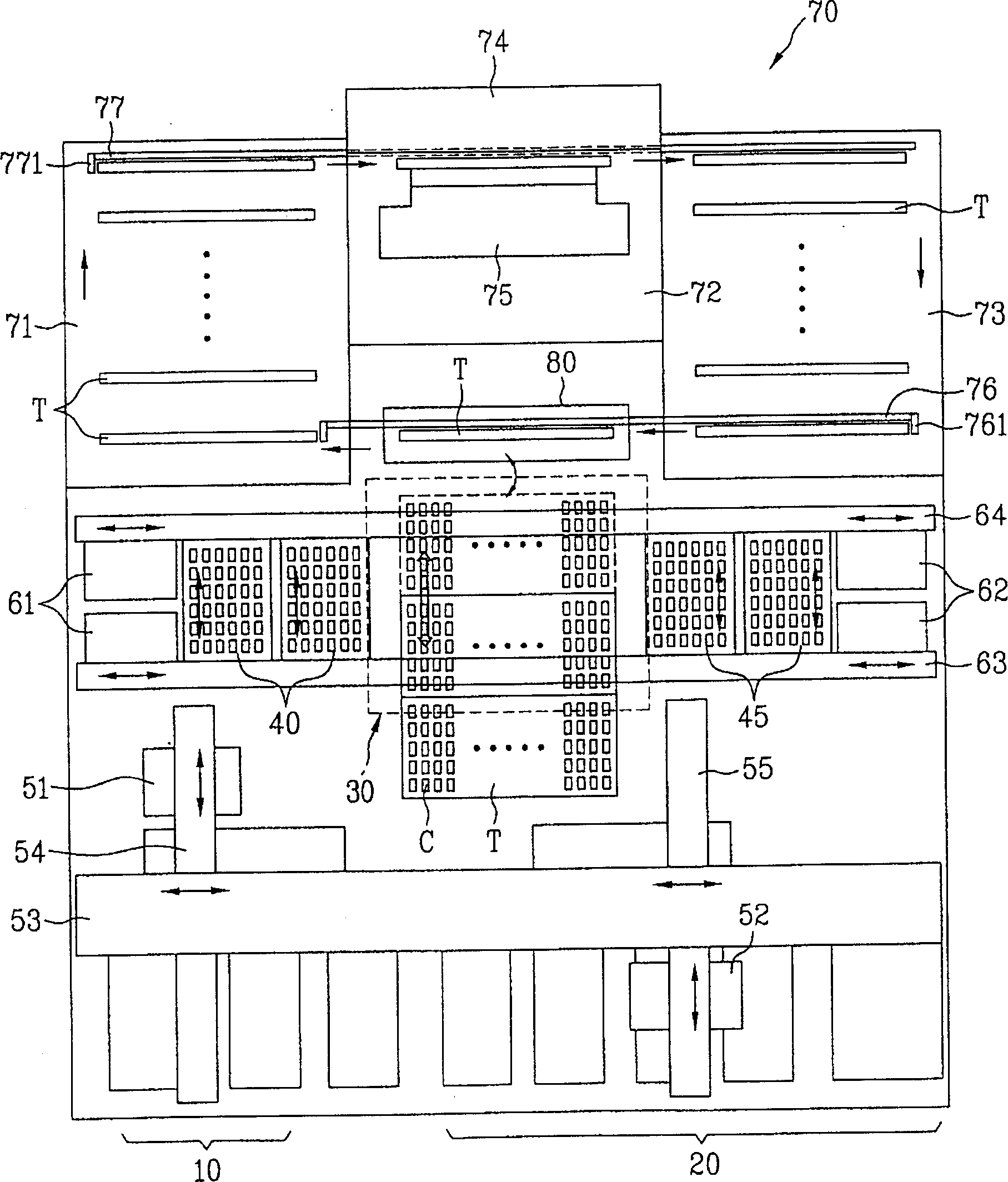
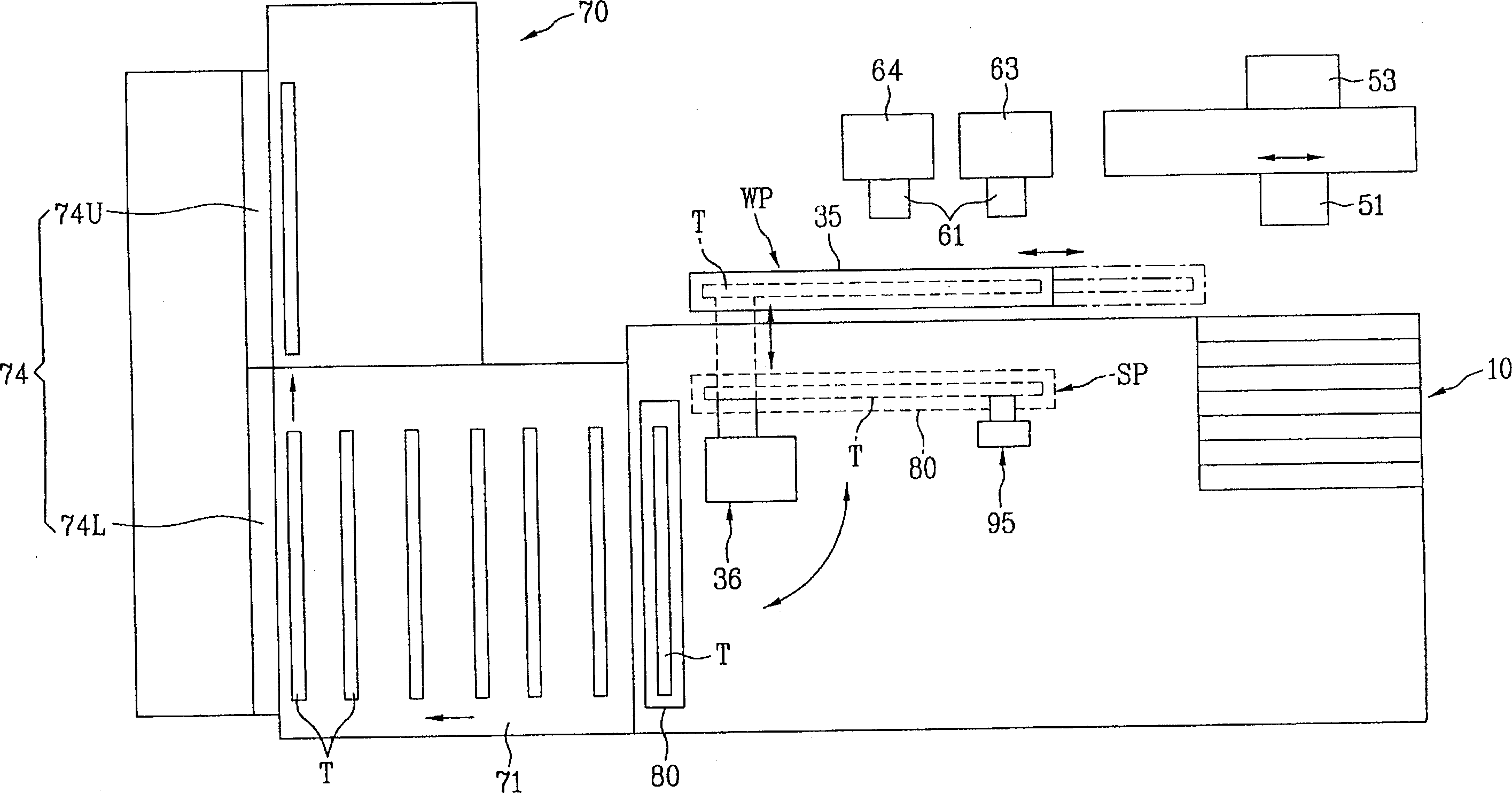
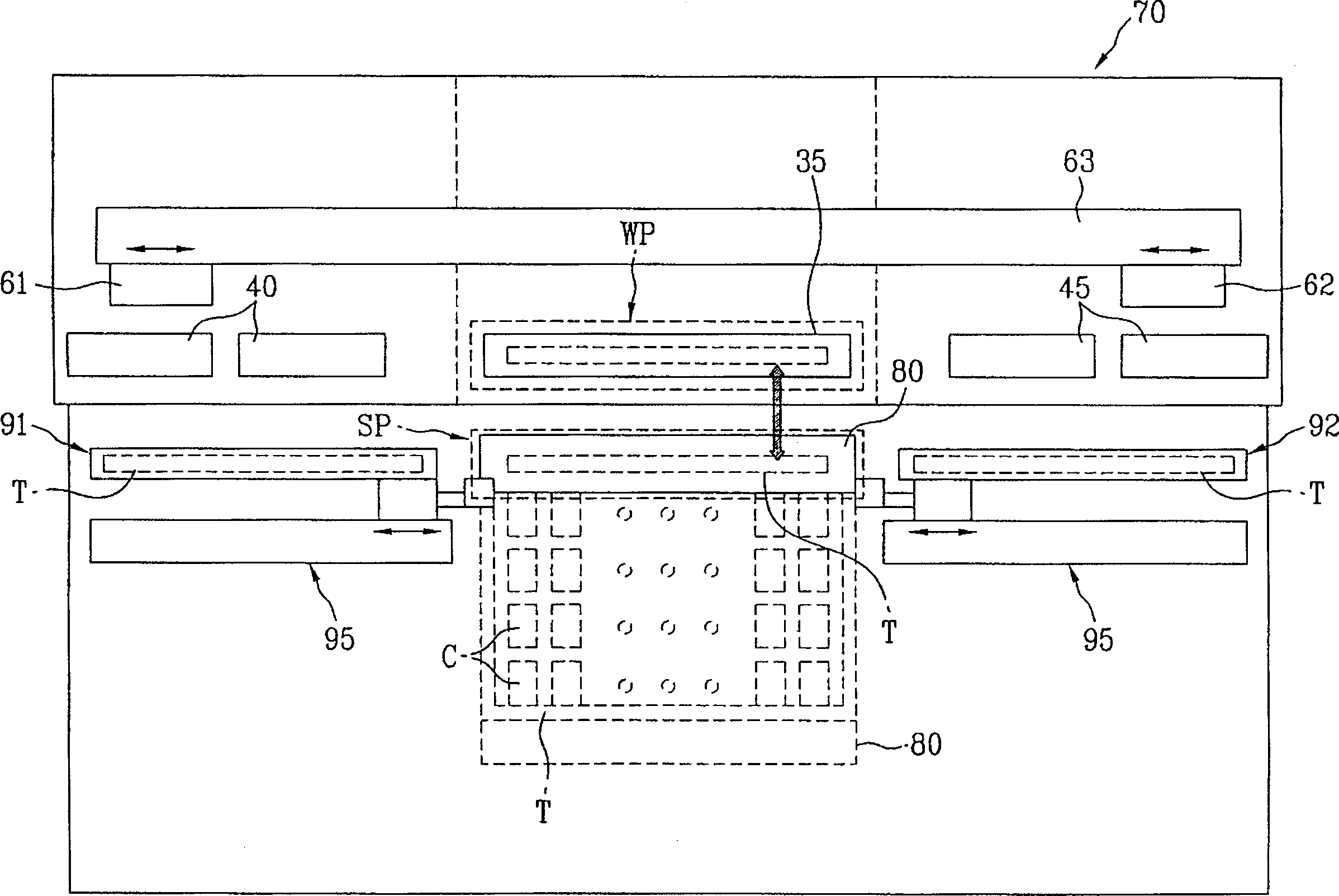
[0046] Figure 1 to Figure 4 A handler for testing semiconductor devices according to one embodiment of the present invention is schematically represented. The processor comprises a loading station 10 mounted at the front of the processor. User trays receiving a plurality of semiconductor devices to be tested are stacked in the loading station 10 . The processor also includes an unloading station 20 disposed on one side of the loading station 10 . In the unloading station 20 , the tested semiconductor devices are sorted according to the test results, and then are received by the user tray in the unloading station 20 according to the sorting results.

[0047] A plurality of buffers 40 and 45 are provided on...


PUM


Abstract

A handler for testing semiconductor devices is disclosed which is capable of simplifying the process carried out in an exchanging station, namely, the process of loading / unloading semiconductor devices in / from test trays, and greatly increasing the number of simultaneously testable semiconductor devices. The handler includes a loading station, an unloading station, test trays, an exchanging station comprising a horizontal moving unit for horizontally moving a selected one of the test trays by a predetermined pitch at a working place, a test station in which at least one test board having a plurality of test sockets to be electrically connected with semiconductor devices is mounted, the test station performing a test while connecting the semiconductor devices in one of the test trays, which is fed from the exchanging station to the test station, to the test sockets, device transfer units for transfer the semiconductor devices between the loading station and the exchanging station and between the exchanging station and the unloading station, respectively, and a tray transfer unit for transfer the test trays between the exchanging station and the test station.

Description

[0001] This application claims priority from Korean Patent Applications 2004-23621 and 2004-23622, both of which were filed on March 22, 2004, the entire contents of which are hereby incorporated by reference. technical field [0002] The present invention relates to a processor for testing semiconductor devices, in particular to a processor for testing semiconductor devices that connects semiconductor devices to test sockets. The test sockets are connected to external testing equipment so that semiconductor devices can be tested, and based on the test Classify the tested semiconductor devices according to the results, and then store the classified semiconductor devices. Background technique [0003] Typically, memory or non-memory semiconductor devices or modular ICs, each containing memory or non-memory components suitably arranged on a substrate to form a circuit, are subjected to various tests after fabrication and before shipment. Semiconductor device. Such testing req...

Claims


Application Information

Patent Timeline
Patent Type & Authority Applications(China)
IPC IPC(8): G01R31/26G01R31/28H01L21/66H01L21/00H01L21/68
CPCG01R31/2601
Inventor 咸哲镐宋镐根朴龙根林祐永徐载奉
Owner MIRAE CORPORATION
Why Eureka
Try Eureka