
Flash memory loading method and system based on boundary scan
A boundary scan and flash memory technology, which is applied in the direction of program loading/starting, information storage, static memory, etc., can solve the problem of incompatibility between loading speed and loading resources occupied by loading, loading stability, etc., to improve transmission efficiency and loading speed, Effect of reducing the number of times data is transferred
- Summary
- Abstract
- Description
- Claims
- Application Information
AI Technical Summary
Problems solved by technology
Method used
Image

Examples
example 1
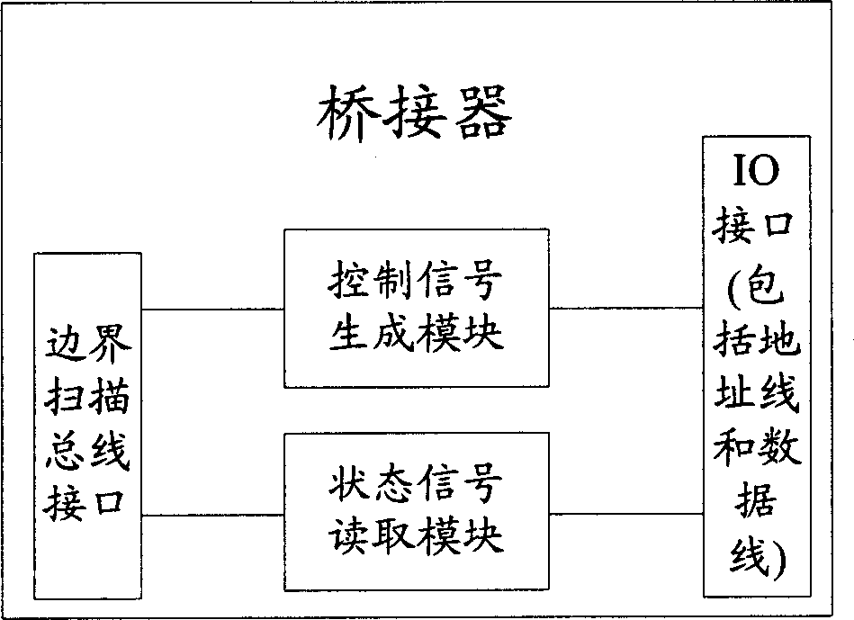
[0055] Example 1 of the bridge: the bridge has a sufficient number of IO interfaces (that is, enough to meet the number requirements of address lines and data lines of the flash memory).
[0056] see image 3 As shown, the bridge includes: a JTAG bus interface, an IO interface, and a control signal generation module and a status signal reading module respectively connected to the JTAG bus interface and the IO interface.
[0057] The JTAG bus interface connects the bridge to the JTAG bus.
[0058] IO interface, used to exchange data with external flash memory.
[0059] The control signal generation module is used to receive instructions from the JTAG bus through the JTAG bus interface, generate control signals correspondingly according to the instructions, and output them through the IO interface.
[0060] The state signal reading module is used to receive the instructions sent by the JTAG bus through the JTAG bus interface, and read the corresponding state signal of the exte...
example 2
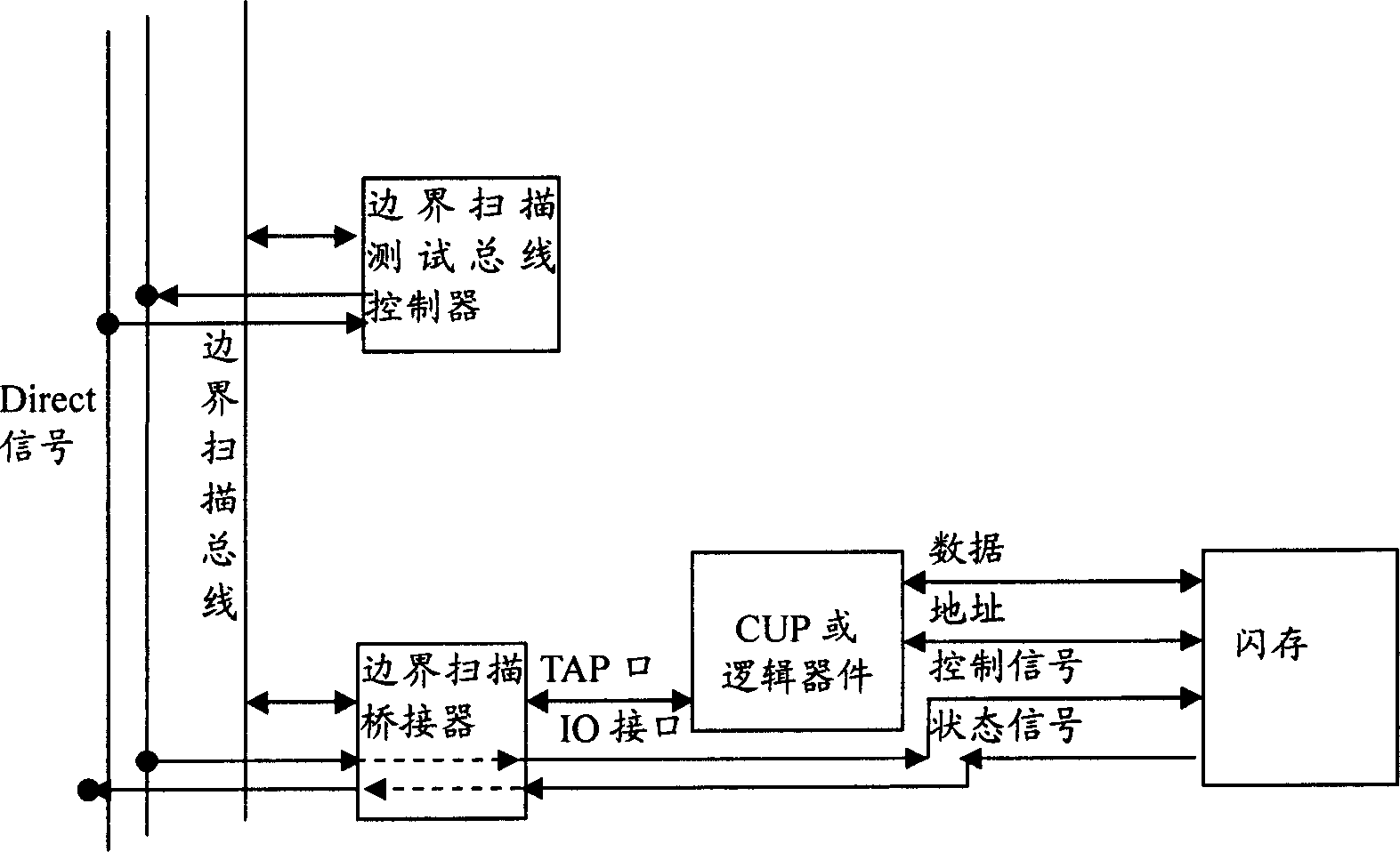
[0070] System Example 2: The bridge does not have a sufficient number of IO interfaces (that is, insufficient to meet the requirements for the number of address lines and data lines of the flash memory).
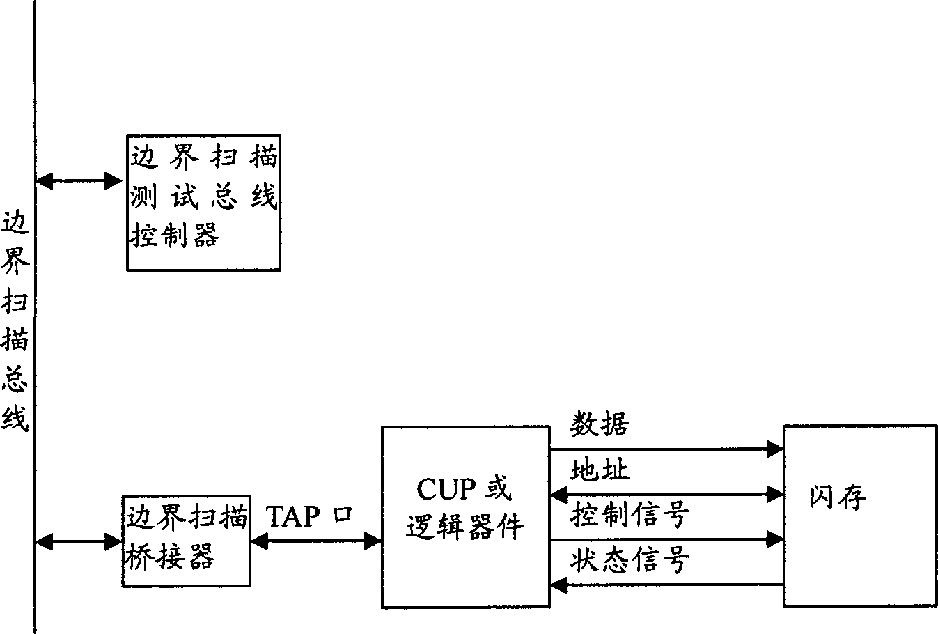
[0071] see Image 6 As shown, the system includes: JTAG bus, JTAGTBC and JTAG Bridge connected with the JTAG bus, and the flash memory to be loaded connected with the JTAG Bridge; the flash memory to be loaded is also connected with the CPU or logic device Connected to the above JTAG Bridge.
[0072] The flash memory to be loaded includes: a data read-write interface, an address read-write interface, a control signal input interface and a state signal output interface. Because the IO interface quantity of JTAG Bridge is insufficient in this example, so this example also includes: CPU or logic device, it is connected with the data read-write interface and the address read-write interface of the flash memory to be loaded, and through TAP interface and described The JTAG Brid...
PUM
 Abstract
Description
Claims
Application Information