Safety writing method for flash memory

A flash memory and security technology, applied in the field of safe reading and writing of chip memory, to achieve good power-down protection, improve system performance, and improve service life.

Active Publication Date: 2006-10-11
FEITIAN TECHNOLOGIES
View PDF0 Cites 24 Cited by
  • Summary
  • Abstract
  • Description
  • Claims
  • Application Information

AI Technical Summary

Problems solved by technology

This is unacceptable in embedded system

Method used


Image

  • Safety writing method for flash memory
  • Safety writing method for flash memory
  • Safety writing method for flash memory

Examples


Embodiment 1

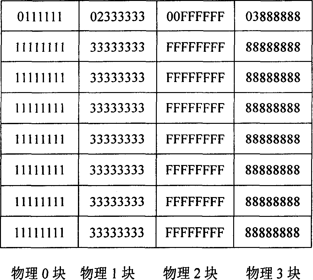
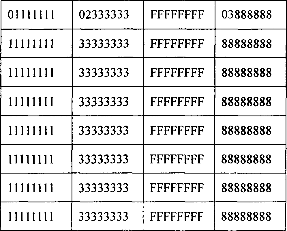
[0049]Embodiment 1, when the flash memory is initialized or formatted by the system, each physical erasing unit in the flash memory is corresponding to a logical block, and each logical block is numbered. In this embodiment, the first block of each logical block is occupied. The byte stores the logical block number, such as figure 1 As shown, the available capacity of each logical block actually becomes 63 bytes, and the size of the entire storage area is 252 bytes. Here we define the logic numbers of the four logic blocks as 00, 01, 02, and 03 respectively, among which the logic block with the logic number 00 is a reserved backup logic block, and it is an unused or erased logic block. for data transfer. At the same time, we set logical block No. 01 to correspond to physical block 0, logical block No. 02 to physical block 1, logical block No. 03 to physical block 3, logical block No. 00 to physical block 2, and the logical addresses to be logical block numbers from small to l...

Embodiment 2

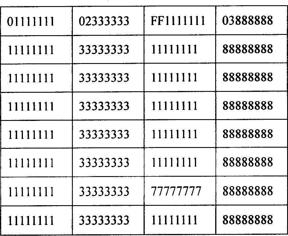
[0060] Embodiment 2, when the flash memory is initialized or formatted by the system, each physical erasing and writing unit in the flash memory is corresponding to a logical block, and each logical block is numbered. In this embodiment, the first one of each logical block is occupied. The byte stores the logical block number, such as Figure 6 As shown, the available capacity of each logical block actually becomes 63 bytes, and the size of the entire storage area is 252 bytes. Here we respectively define the logical numbers of the four logical blocks as 01, 02, 03, and FF, and the logical block with the logical block number of FF is a reserved backup logical block for data transfer. At the same time, we set logical block No. 01 to correspond to physical block 0, logical block No. 02 to physical block 1, logical block No. 03 to physical block 3, and logical block No. FF to physical block 2. The number of logical blocks is determined according to specific applications. Differe...


PUM


Abstract

The invention relates to a method for safely reading and writing chip memory, especially relating to flash memory. The invention defines each minimum rub unit as one logic block, while each logic contains one or several logic pages; and via numbering each logic block, writes the data and the content of target logic block into backup logic block; then exchanges the logic number of backup logic block with the block number of target logic block, to realize safely reading and writing data, with better power cut protection function; and since said backup block is random, it can avoid one rub block being over rubbed, to reach maximum rub times quicker than other logic block, to realize rub balance and improve the service life of flash memory, to improve the system property. Compared to present technique, it can avoid rubbing whole rub block usually to reduce the cost of memory.

Description

technical field [0001] The invention relates to a method for safely reading and writing chip memory, in particular to a method for safely writing flash memory. technical background [0002] In recent years, flash memory (Flash Memory) storage media has been rapidly developed and widely used in embedded systems. Flash memory is a kind of semiconductor-based memory, which has the functions of retaining internal information after the system is powered off, and online erasing. It is a new type of memory that replaces the original EEPROM storage medium. [0003] First, let’s introduce the characteristics and limitations of flash memory (Flash Memory). The characteristics and limitations of flash memory introduced here are all from the perspective of the upper file system, and will not involve specific physical characteristics: [0004] A) The smallest addressing unit of flash memory is byte (byte), not sector (sector) on the disk. This means that we can read data from any offse...

Claims


Application Information

Patent Timeline
IPC IPC(8): G06F12/02G06F11/14
Inventor 陆舟于华章
Owner FEITIAN TECHNOLOGIES
Why Eureka
Try Eureka