Active component and switch circuit device

A technology of active components and switching circuits, applied in circuits, electrical components, electric solid-state devices, etc., can solve problems such as degradation of high-frequency characteristics

Inactive Publication Date: 2006-11-01
SANYO ELECTRIC CO LTD
View PDF1 Cites 11 Cited by
  • Summary
  • Abstract
  • Description
  • Claims
  • Application Information

AI Technical Summary

Problems solved by technology

However, if the emission ballast resistor and the base ballast resistor are inserted, there will be a problem that the high-frequency characteristics will be degraded.

Method used


Image

  • Active component and switch circuit device
  • Active component and switch circuit device
  • Active component and switch circuit device

Examples


Embodiment Construction

[0115] Next, use Figure 1 to Figure 25 Embodiments of the present invention will be described in detail.

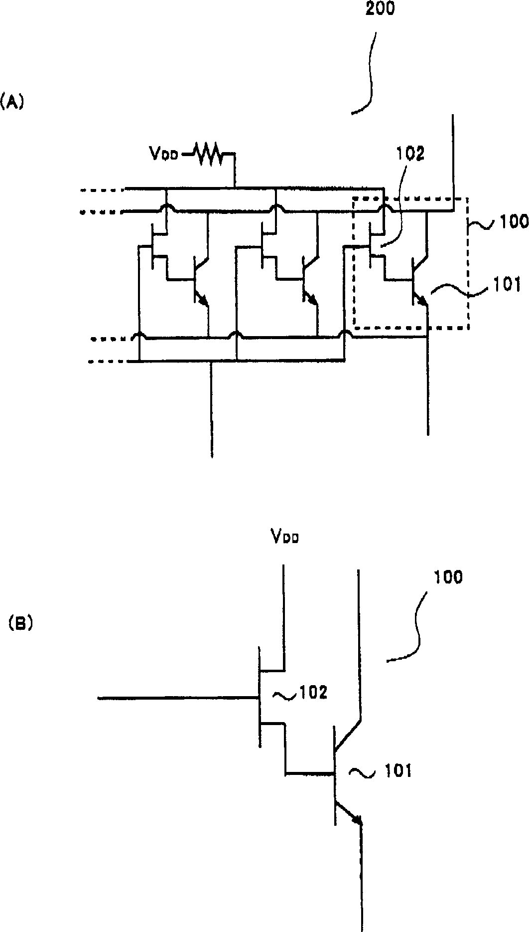
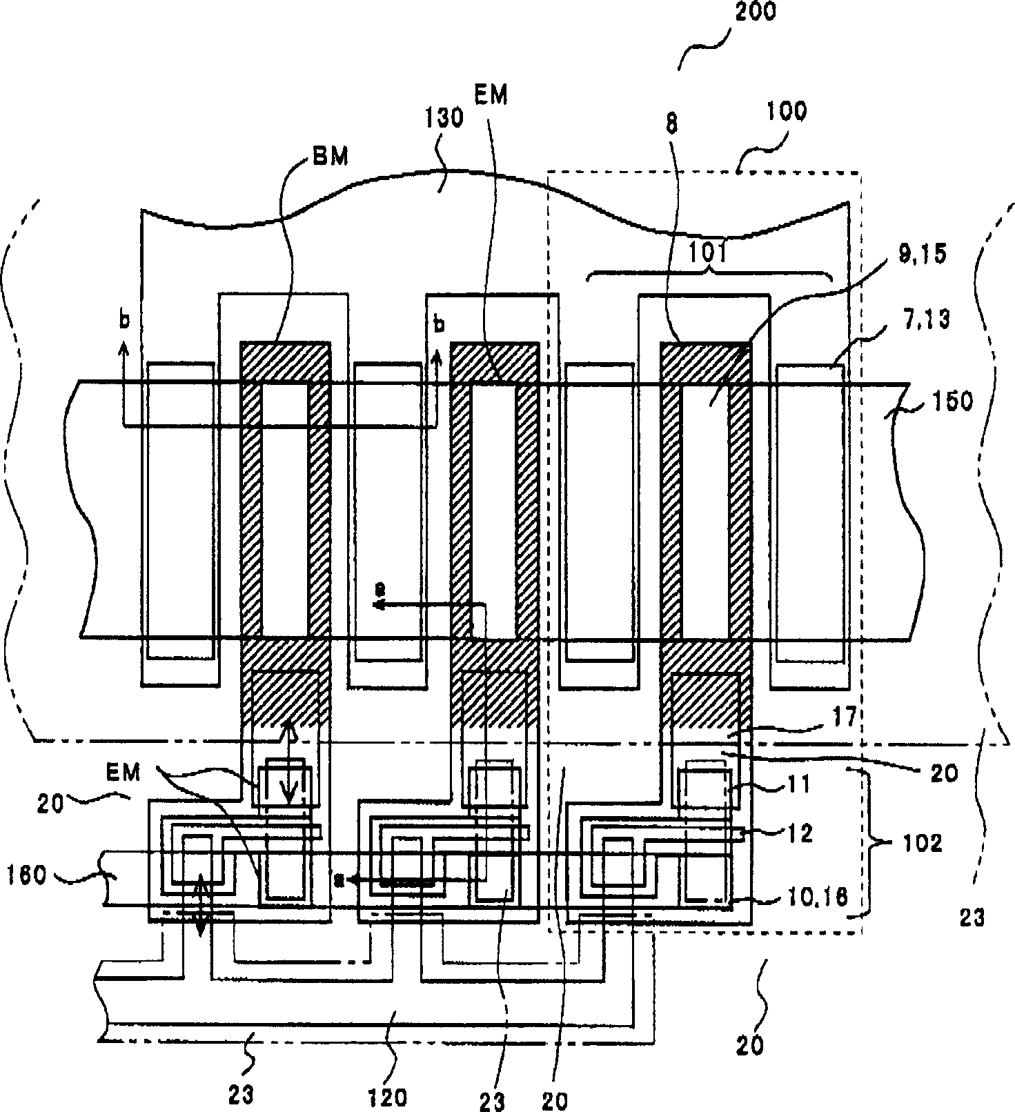
[0116] First, refer to Figure 1 to Figure 5 , represents the active element of the first embodiment of the present invention. figure 1 (A) is the circuit diagram of the active components, figure 1 (B) is a circuit diagram of a unit element constituting an active element.

[0117] Such as figure 1 (A), the active element 200 is a structure in which a plurality of unit elements 100 (dotted line) are connected in parallel. The unit cell 100 has a first transistor 101 and a second transistor 102 .

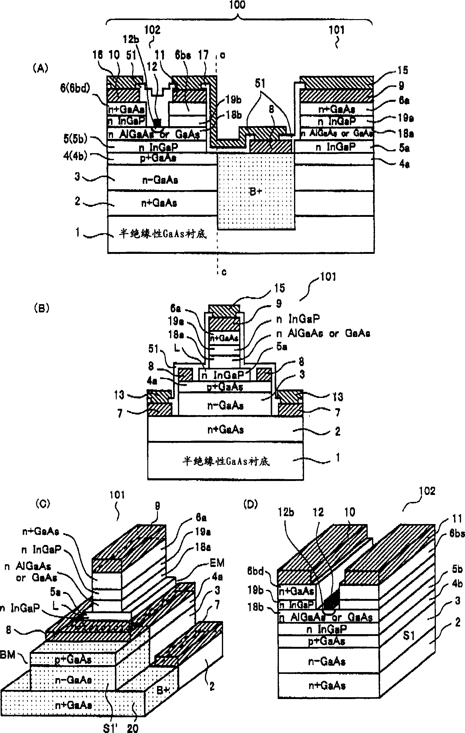
[0118] The first transistor 101 forms at least one heterojunction by laminating semiconductor layers serving as a collector layer, a base layer, and an emitter layer on a compound semiconductor substrate, and has a collector, a base, and a semiconductor layer respectively connected to each semiconductor layer. emitter of the HBT. The HBT has a mesa structure. In this e...


PUM


Abstract

A unit HBT and a unit FET are arranged to be adjacent to each other through an isolation region and a base electrode of the unit HBT is connected to a source electrode of the unit FET to form a unit element, and a plurality of unit elements are connected to form an active element. This makes it possible to implement the active element in which a current is not likely to concentrate on the unit element and no destruction is generated by the second breakdown. Moreover, although a buried gate electrode structure is used to ensure a withstand pressure in the unit FET, a buried portion is structured not to be diffused to an InGaP layer, and thereby it is possible to prevent Pt from being abnormally diffused. Furthermore, a selection etching can be used for a formation of an emitter mesa, that of a base mesa, that of a ledge in the unit HBT, and a gate recess etching in the unit FET, and a good reproducibility can be obtained.

Description

technical field [0001] The invention relates to an active element and a switch circuit device with a heterojunction bipolar transistor, in particular to a temperature compensation type active element and a switch circuit device. Background technique [0002] Heterojunction Bipolar Transistor (Heterojunction Bipolar Transistor: hereinafter referred to as HBT) has a higher emission efficiency and a current amplification factor of h FE Large, so the base concentration can be greatly increased, and the transistor operation can be performed uniformly throughout the base. As a result, compared with GaAs MESFET (Metal Semiconductor Field Effect Transistor: Metal Semiconductor Field Effect Transistor), GaAs JFET (Junction FET: Junction Field Effect Transistor), and HEMT (High Electron Mobility Transistor: High Electron Mobility Transistor), It has high current density and low connection resistance, so it has good efficiency, gain, and distortion characteristics. [0003] High-effi...

Claims


Application Information

Patent Timeline
Patent Type & Authority Applications(China)
IPC IPC(8): H01L27/06
Inventor 浅野哲郎
Owner SANYO ELECTRIC CO LTD
Why Eureka
Try Eureka