Dielectric film layer structure and fabricating method thereof

a technology of dielectric film and fabrication method, which is applied in the direction of fixed capacitor details, stacked capacitors, fixed capacitors, etc., can solve the problem of insufficient voltage output uniformity of display devices, and achieve the effect of reducing the influence of voltage drop, less charges, and improving panel voltage output uniformity

Active Publication Date: 2020-06-25
WUHAN CHINA STAR OPTOELECTRONICS SEMICON DISPLAY TECH CO LTD
View PDF0 Cites 0 Cited by
  • Summary
  • Abstract
  • Description
  • Claims
  • Application Information

AI Technical Summary

Benefits of technology

[0048]Beneficial effects of the present disclosure are that: in an embodiment of the present disclosure, SiNx and SiOx are used as material of the capacitor dielectric layer, and a ratio of SiNx in the capacitor dielectric layer increases along a signal transmission direction, and a ratio of SiOx in the capacitor dielectric layer decreases along the signal transmission direction. Since a dielectric constant of SiNx is larger than that of SiOx, in a place where voltage drop is relatively large, the dielectric layer is mainly made of SiNx to store more charges, and a capacitor charges a relatively large amount of current to thin film transistors, causing the thin film transistors to be in a high voltage state. In a place where voltage drop is relatively small, the dielectric layer is mainly made of SiOx to store less charges, and the capacitor charges a relatively small amount of current to the thin film transistors, causing the thin film transistors to be in a low voltage state, thereby changing current for charging thin film transistors, reducing influence of the voltage drop, and improving uniformity of panel voltage output.

Problems solved by technology

Due to the metal having resistance, as a transmission distance increases, voltage will decrease, i.e., the voltage away from a signal input terminal is smaller than the voltage close to the signal input terminal, resulting in insufficient voltage output uniformity of the display device.

Method used


Image

  • Dielectric film layer structure and fabricating method thereof
  • Dielectric film layer structure and fabricating method thereof
  • Dielectric film layer structure and fabricating method thereof

Examples


embodiment 1

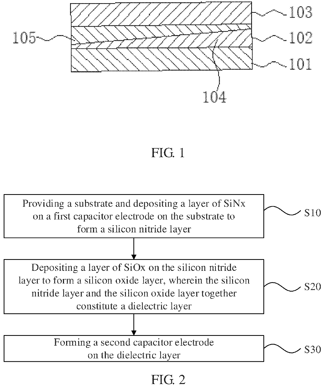
[0057]An embodiment of the present disclosure provides a dielectric film layer structure. As shown in FIG. 1, FIG. 1 is a structural schematic diagram of a dielectric film layer according to the present embodiment. The dielectric film layer structure includes a first capacitor electrode 101, a dielectric layer 102 disposed on the first capacitor electrode 101, a second capacitor electrode 103 disposed on the dielectric layer 102, wherein the first capacitor electrode 101, the dielectric layer 102, and the second capacitor electrode 103 together constitute a storage capacitor of a display panel.

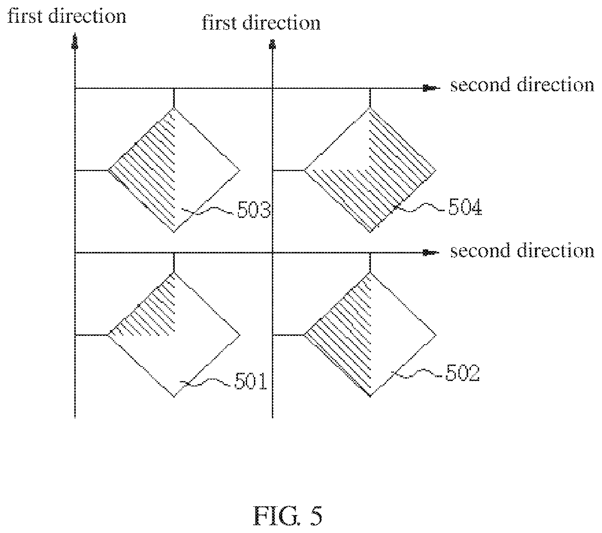
[0058]In the present embodiment, the dielectric layer 102 consists of silicon nitride layer 104 and a silicon oxide layer 105, wherein a ratio of SiNx in the dielectric layer increases along a first direction and a second direction, and a ratio of SiOx in the dielectric layer decreases along the first direction and the second direction. Because a dielectric constant of SiNx is greater than a d...

embodiment 2

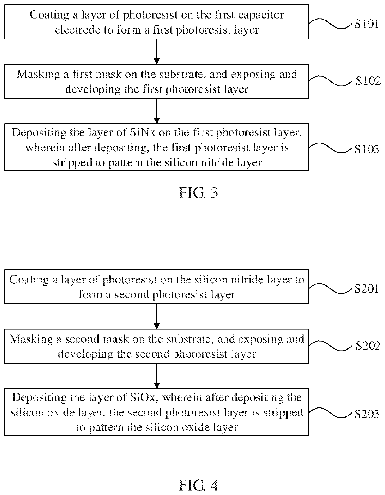
[0066]In the present embodiment, as shown in FIG. 3, the step S10 further comprises:[0067]a step S101 of coating a layer of photoresist on the first capacitor electrode 101 to form a first photoresist layer;[0068]a step S102 of masking a first mask on the substrate, and exposing and developing the first photoresist layer; and[0069]a step S103 of depositing the layer of SiNx on the first photoresist layer, wherein after depositing the silicon nitride layer, the first photoresist layer is stripped to pattern the silicon nitride layer 104.

[0070]In the present embodiment, as shown in FIG. 4, the step S20 further comprises:[0071]a step S201 of coating a layer of photoresist on the silicon nitride layer 104 to form a second photoresist layer;[0072]a step S202 of masking a second mask on the substrate, and exposing and developing the second photoresist layer; and[0073]a step S203 of depositing the layer of SiOx, wherein after depositing the silicon oxide layer, the second photoresist layer...

embodiment 3

[0079]The present embodiment provides a fabricating method of a dielectric film layer structure. In the present embodiment, the dielectric film layer structure provided by the first embodiment is referred to, and the fabricating method provided by the embodiment is described in detail below with reference to FIG. 1 to FIG. 5.

[0080]As shown in FIG. 2, FIG. 2 is a flowchart of a fabricating method of a dielectric film layer according to the present embodiment. The method comprises:[0081]a step S10 of providing a substrate (not shown) and depositing a layer of SiNx on a first capacitor electrode 101 on the substrate to form a silicon nitride layer 104;[0082]a step S20 of depositing a layer of SiOx on the silicon nitride layer 104 to form a silicon oxide layer 105, wherein the silicon nitride layer 104 and the silicon oxide layer 105 together constitute a dielectric layer 102; and[0083]a step S30 of forming a second capacitor electrode 103 on the dielectric layer 102,[0084]wherein a rat...


PUM

PropertyMeasurementUnit
dielectricaaaaaaaaaa
transparentaaaaaaaaaa
areaaaaaaaaaaa

Abstract

A dielectric film layer structure and a fabricating method thereof are provided. The dielectric film layer structure at least has a first capacitor electrode, a dielectric layer, and a second capacitor electrode, wherein the dielectric layer includes two materials of SiNx and SiOx. In a place where voltage drop is relatively large, the dielectric layer is mainly made of SiNx, and in a place where the voltage drop is relatively small, the dielectric layer is mainly made of SiOx, thereby changing current for charging thin film transistors, reducing influence of the voltage drop, and improving uniformity of panel voltage output.

Description

FIELD OF DISCLOSURE[0001]The present disclosure relates to display device fabrication, and more particularly, to a dielectric film layer structure and a fabricating method thereof.BACKGROUND OF DISCLOSURE[0002]There are many display pixels on display devices. In order to save a huge hardware drive circuit, a matrix type structure is implemented. That is, electrodes of a set of horizontal display pixels are connected together and referred to as row electrodes, and segment electrodes of a set of vertical display pixels are connected together and referred to as column electrodes. Each of the display pixels on the display device is determined by positions in a column and a row at which it is located. In a driving method, a raster scanning method is adopted correspondingly. A dynamic driving method of the display device applies a selection pulse to the row electrodes through a scan line loop, and all the column electrodes displaying data give corresponding selective or non-selective driv...

Claims


Application Information

Patent Timeline
Patent Type & Authority Applications(United States)
IPC IPC(8): H01G4/30H01G4/12H01L27/12
CPCH01L27/1255H01G4/306H01G4/129H01L27/1259H01L28/40H01L27/0288H01L27/0629
Inventor ZHAO, KAIXIANG
Owner WUHAN CHINA STAR OPTOELECTRONICS SEMICON DISPLAY TECH CO LTD
Why Eureka
Try Eureka