Method for producing semiconductor imaging sensor by organic coating

An image sensor and organic coating technology, used in the field of manufacturing semiconductor image sensors, can solve problems such as poor development, affecting color pixel performance, excessive noise, etc. The effect of improving device performance

Inactive Publication Date: 2010-05-12
SHANGHAI INTEGRATED CIRCUIT RES & DEV CENT +1
View PDF5 Cites 0 Cited by
  • Summary
  • Abstract
  • Description
  • Claims
  • Application Information

AI Technical Summary

Problems solved by technology

However, the use of negative photoresist will be accompanied by some side effects and adverse reactions, such as photoresist bottom plate residue, photoresist surface residue, photoresist swelling after development, photoresist pattern outline slightly deformed, etc.
Among them, the photoresist bottom plate residue and surface residue are particularly fatal. The photoresist residue on the substrate is caused by the reflected light on the ground, which causes the negative photoresist to be exposed to cross-linking reactions in unnecessary areas, resulting in bottom film residue. Causes too much noise and affects the performance of color pixels; the photoresist residue on the surface of the filter layer is mainly from the lack of development. Due to the hydrophobic nature of the photoresist, the water-soluble developer is affected by the surface tension. It cannot cover the surface of the silicon wafer quickly, relatively well, and evenly, resulting in poor development and ultimately bad results
The residual film will affect the transmission efficiency of the filter layer and the accuracy of the filter layer, which can cause image distortion, color drift and other adverse reactions

Method used


Image

  • Method for producing semiconductor imaging sensor by organic coating
  • Method for producing semiconductor imaging sensor by organic coating
  • Method for producing semiconductor imaging sensor by organic coating

Examples


Embodiment Construction

[0036] The specific implementation of the present invention will be further described in detail below in conjunction with the accompanying drawings.

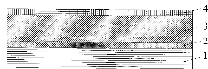
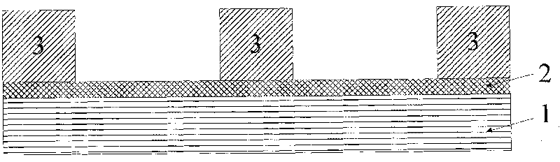
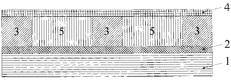
[0037] Firstly, the substrate is cleaned, and a bottom anti-reflection development strengthening layer is coated on the surface of the substrate. The coating thicknesses are 60nm, 70nm, 80nm, 90nm, 100nm, 110nm and 120nm respectively, the baking temperatures are 180°C, 200°C and 220°C respectively, and the baking times are 60 seconds, 70 seconds, 80 seconds and 90 seconds respectively and 100 seconds, by coating the bottom anti-reflective development strengthening layer to reduce the reflected light of the base and enhance the development performance.

[0038] Next, coat the red light pixel semiconductor image sensor filter layer material on the bottom organic material, the coating thickness is 1000nm, 1100nm, 1200nm, 1300nm, 1400nm or 1500nm, and the baking temperature is 180°C, 200°C or 220°C , the time is 60 seconds, 70 seco...


PUM


Abstract

The process provided for fabricating semiconductor image sensor using an organic coating comprises: an anti-reflection property of said organic coating at top surface and bottom surface is used to reduce the intensity of reflected light on a substrate so as to reduce the residues of substrate film generated by cross bounding of negative photoresist containing filter material due to parasitic light; meanwhile a surface developing activator contained in said organic coating is used to optimize the developing art and to reduce the residues of film on the top.

Description

technical field [0001] The invention belongs to the technical field of integrated circuit technology, and in particular relates to a method for manufacturing a semiconductor image sensor by using an organic coating. Background technique [0002] With the continuous improvement of integrated circuit manufacturing technology, the volume of semiconductor devices is becoming smaller and smaller. At the same time, ultra-large-scale or even ultra-large-scale chips, high integration and densification make it possible to realize multi-functions on a single chip. The current semiconductor industry is developing towards diversification, multi-function and continuous development. Semiconductor image sensor is one of the trends. The semiconductor image sensor is mainly composed of a microscopic fly eye lens, a color filter layer, a photosensitive photodiode or a complementary metal oxide semiconductor device and an image processor. The basic principle is to use the filter characterist...

Claims


Application Information

Patent Timeline
Patent Type & Authority Patents(China)
IPC IPC(8): H01L27/146
Inventor 朱骏
Owner SHANGHAI INTEGRATED CIRCUIT RES & DEV CENT
Why Eureka
Try Eureka