Method and apparatus for depositing tungsten after surface treatment to improve film characteristics

a technology of surface treatment and tungsten, which is applied in the direction of chemical vapor deposition coating, solid-state devices, coatings, etc., can solve the problems of reducing the deposition rate of tungsten by at least one order of magnitude, the need for more complex chamber design and gas flow techniques, and the difficulty of traditional cvd methods for depositing tungsten, etc., to improve the surface mobility of adsorption chemical species, improve the step coverage and resistivity of the tungs

Inactive Publication Date: 2005-08-30
APPLIED MATERIALS INC
View PDF206 Cites 128 Cited by
  • Summary
  • Abstract
  • Description
  • Claims
  • Application Information

AI Technical Summary

Benefits of technology

[0011]A method and system to form a refractory metal layer over a substrate includes introduction of a reductant, such as PH3 or B2H6, followed by introduction of a tungsten containing compound, such as WF6, to form a tungsten layer. It is believed that the reductant reduces the fluorine content of the tungsten layer while improving the step coverage and res...

Problems solved by technology

These requirements become more critical as substrate size increases (e.g., from 200 mm diameter substrates to 300 mm substrates), creating a need for more complexity in chamber design and gas flow technique to maintain adequate uniformity.
A drawback with ALD techniques is that the deposition rate is much lower than typical CVD techniques by at least one order of magnitude.
Depositing tungsten by traditional CVD methods, however, is attendant with several disadvantages.
For example, blanket deposition of a tungsten layer on a semiconductor wafer is time-consuming at temperatures below 400° C. The deposition rate of tungsten may be imp...

Method used


Image

  • Method and apparatus for depositing tungsten after surface treatment to improve film characteristics
  • Method and apparatus for depositing tungsten after surface treatment to improve film characteristics
  • Method and apparatus for depositing tungsten after surface treatment to improve film characteristics

Examples


Embodiment Construction

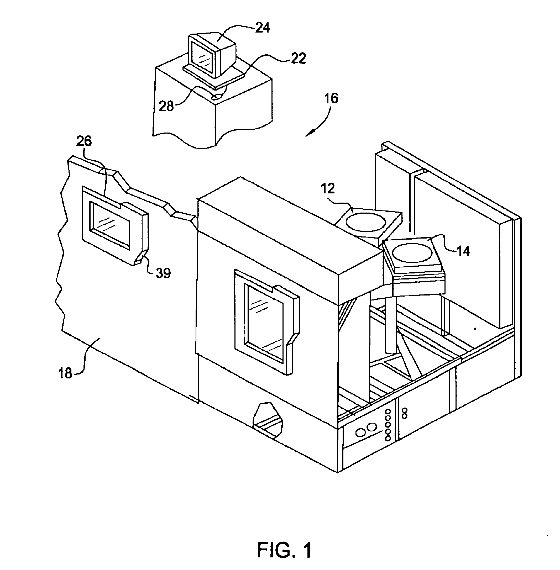
[0031]Referring to FIG. 1, an exemplary wafer processing system includes one or more processing chambers 12 and 14 disposed in a common work area 16 surrounded by a wall 18. Processing chambers 12 and 14 are in data communication with a controller 22 that is connected to one or more monitors, shown as 24 and 26. The monitors typically display common information concerning the process associated with processing chambers 12 and 14. One of the monitors 26 is mounted on wall 18, with the remaining monitor 24 being disposed in work area 16. Operational control of processing chambers 12 and 14 may be achieved by the use of a light pen, associated with one of the monitors 24 and 26, to communicate with controller 22. For example, light pen 28 is associated with monitor 24 and facilitates communication with controller 22 through monitor 24. Light pen 39 facilitates communication with controller 22 through monitor 26.

[0032]Referring both to FIGS. 1 and 2, each of processing chambers 12 and 1...


PUM


Abstract

A method and system to form a refractory metal layer over a substrate includes introduction of a reductant, such as PH3 or B2H6, followed by introduction of a tungsten containing compound, such as WF6, to form a tungsten layer. It is believed that the reductant reduces the fluorine content of the tungsten layer while improving the step coverage and resistivity of the tungsten layer. It is believed that the improved characteristics of the tungsten film are attributable to the chemical affinity between the reductants and the tungsten containing compound. The chemical affinity provides better surface mobility of the adsorbed chemical species and better reduction of WF6 at the nucleation stage of the tungsten layer. The method can further include sequentially introducing a reductant, such as PH3 or B2H6, and a tungsten containing compound to deposit a tungsten layer. The formed tungsten layer can be used as a nucleation layer followed by bulk deposition of a tungsten layer utilizing standard CVD techniques. Alternatively, the formed tungsten layer can be used to fill an aperture.

Description

CROSS-REFERENCE TO RELATED APPLICATIONS[0001]This application claims benefit of U.S. Provisional Patent Application Ser. No. 60 / 305,765, filed Jul. 16, 2001, which is herein incorporated by reference.BACKGROUND OF THE INVENTION[0002]1. Field of the Invention[0003]Embodiments of the invention relate to the processing of semiconductor substrates. More particularly, embodiments of the invention relate to improvements in the process of depositing refractory metal layers on semiconductor substrates.[0004]2. Description of the Related Art[0005]The semiconductor processing industry continues to strive for larger production yields while increasing the uniformity of layers deposited on substrates having larger surface areas. These same factors in combination with new materials also provide higher density of circuits per unit area of the substrate. As circuit density increases, the need for greater uniformity and process control regarding layer thickness rises. As a result, various technologi...

Claims


Application Information

Patent Timeline
IPC IPC(8): C23C16/06C23C16/14H01L21/285H01L21/02H01L21/70H01L21/768C23C16/44C23C16/455H01L21/28
CPCC23C16/0281C23C16/14C23C16/45525C23C16/45529H01L21/28562H01L21/76843H01L21/76876H01L21/76877H01L2221/1089
Inventor BYUN, JEONG SOO
Owner APPLIED MATERIALS INC
Why Eureka
Try Eureka