

Method for cleaning semiconductor wafer
A semiconductor and wafer technology, applied in the new cleaning field, can solve the problems of high rejection rate of wafers, difficult to clean, unable to achieve cleaning effect, etc., to achieve the effect of eliminating defects and reducing rejection rate
- Summary
- Abstract
- Description
- Claims
- Application Information
AI Technical Summary
Problems solved by technology
Method used
Image

Examples
Embodiment Construction
[0021] In order to help understand the present invention, the present invention will be further described in detail below in conjunction with the relevant drawings.
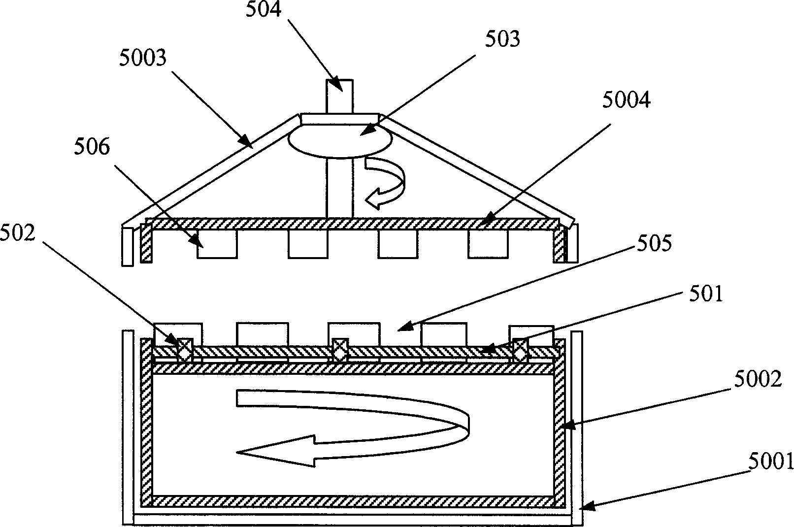
[0022] Figure 4a , Figure 4b A first embodiment of the invention is shown. Such as Figure 4a As shown, a wafer 101 is placed on the bracket 1002 in the shell 1001 of the container 100, the wafer 101 is fixed on the bracket 1002 by pins 102, and the drive shaft 104 of the drive motor 103 passes through the shell 1001 to cooperate with the bracket 1002. Before cleaning, the bracket 1002 and the bracket cover 1004 are snapped together through the engagement of the slot 105 on the bracket 1002 and the buckle 106 on the bracket cover 1004, so that the shell 1001 and the shell cover 1003 are snapped together. When the motor drive shaft 104 was driven by the drive motor 103 to rotate, the drive shaft 104 drove the support 1002 to rotate, so that the wafer 101 on the support 1002 was around its center point O 101 ...
PUM
 Abstract
Description
Claims
Application Information