Eureka AIR delivers breakthrough ideas for toughest innovation challenges, trusted by R&D personnel around the world.

Chip, device using the chip, and method of using the chip

A chip and equipment technology, applied in the field of chips, equipment using the chip, and the equipment using the equipment, can solve the problems of operating sample components, difficulty in using other samples, etc., and achieve the effect of preventing pollution, fast and reliable operation

Inactive Publication Date: 2006-11-22
NEC CORP
View PDF2 Cites 12 Cited by
  • Summary
  • Abstract
  • Description
  • Claims
  • Application Information

AI Technical Summary

Problems solved by technology

[0007] In addition, if the channel located on the chip is covered, it is difficult to replace the sample in the channel with other samples, and it is difficult to directly manipulate the components of the sample from the outside

Method used


Image

  • Chip, device using the chip, and method of using the chip
  • Chip, device using the chip, and method of using the chip
  • Chip, device using the chip, and method of using the chip

Examples


no. 1 example

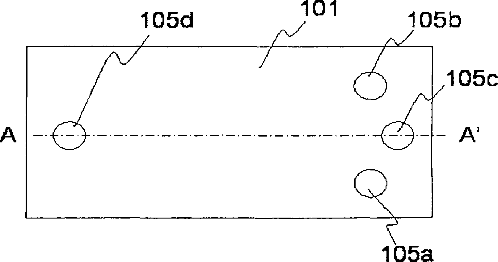
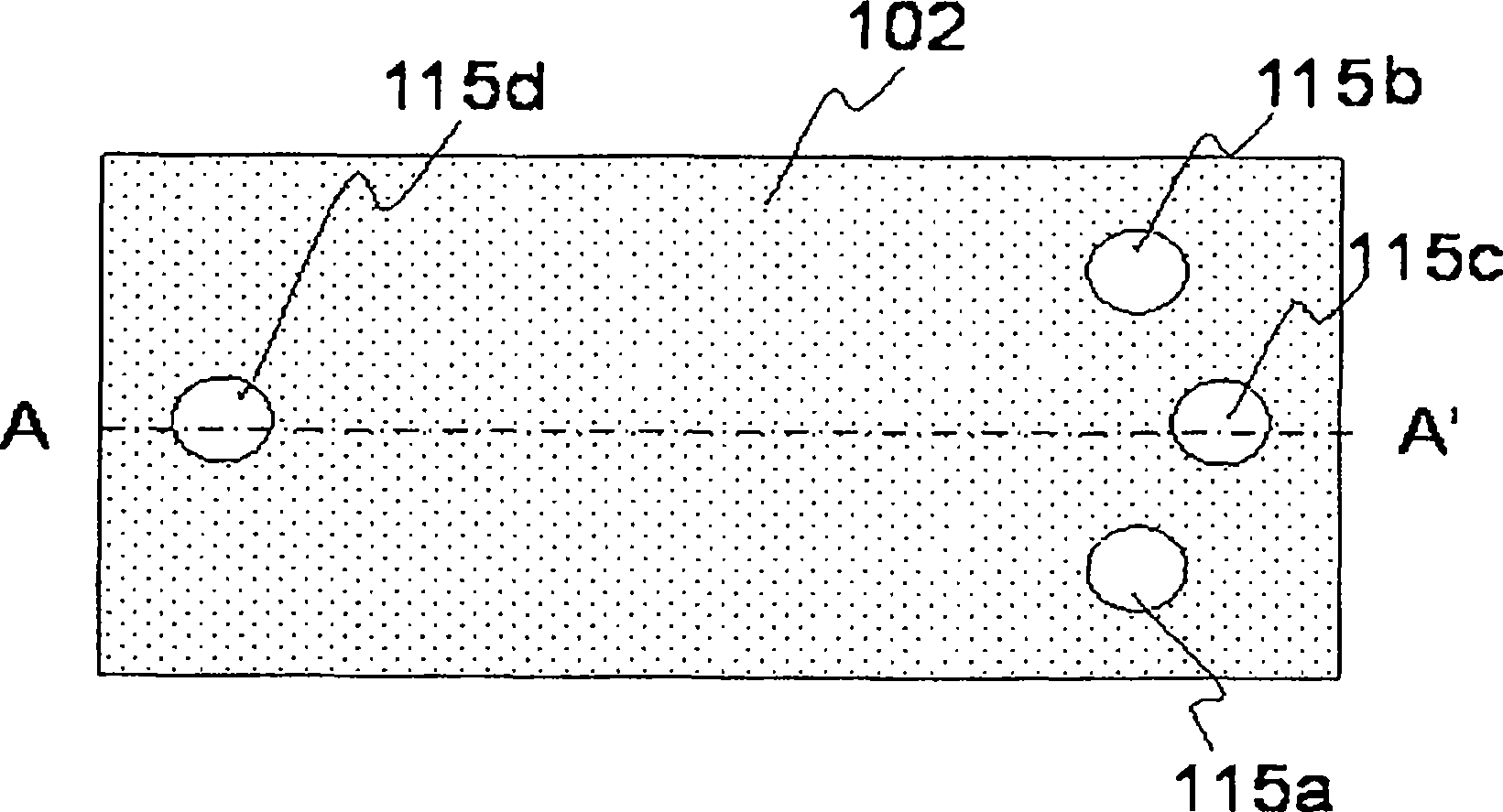
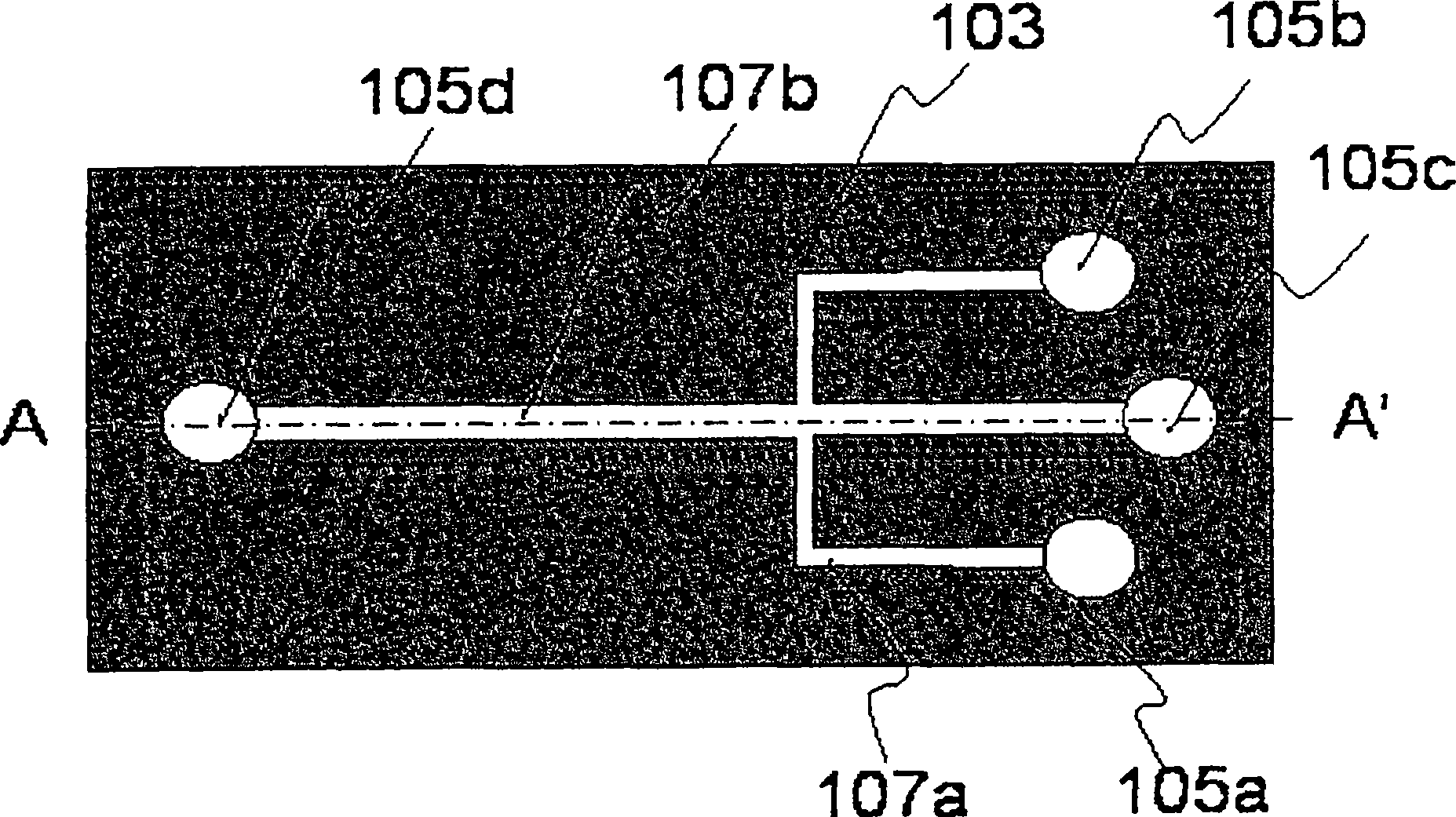
[0134] This embodiment relates to a chip in which a cap covering a channel on the surface of the substrate is attached to the surface of the substrate. Figure 1 to Figure 3 Each figure shows the components of the chip of this embodiment as a top view. Figure 4 for along Figure 1 to Figure 3 The sectional view of the line A-A' in , shows the state that the chip 112 of this embodiment is assembled. Figure 5 is a perspective view showing a state in which the chip 112 of this embodiment is fixed to a fixing device, and Figure 6 for along Figure 5 The cross-sectional view of the line B-B' in. Figure 48 is a diagram showing a device using the chip of this embodiment. Figure 49 is a diagram showing a device using the chip of this embodiment. Refer below Figure 1 to Figure 6 , Figure 48 and 49 The chip of this embodiment will be described.

[0135] Such as Figure 4 As shown, chip 112 includes substrate 103 and lid 113 . The cover 113 includes the resin layer 102 ...

no. 2 example

[0170] The fixing device for fixing the chip 112 described in the first embodiment is not limited to the above structure. For example, pressurization may be performed by hydraulic equipment or the like. Figure 7 is a sectional view showing a state where the chip according to this embodiment is set to a fixing device. Figure 8 It is a top view showing the assembly of the chip and the support plate of the fixture before the cover is placed on the chip.

[0171] The chip 212 of this embodiment is used by being set on the fixed device 208 . The fixture 208 is configured to crimp the lid of the chip 212 to the substrate surface by clamping the upper surface of the lid of the chip 212 . Chip 212 has substrate 201 and plate-shaped cover 205 . Channel 202 and reservoir 203 are formed on substrate 201 . Also, a hole 213 approximately equal in size to the reservoir 203 is located on the reservoir 203 portion of the substrate 201 . For example, when electrophoresis is performed by...

no. 3 example

[0178] This embodiment relates to a pattern in which the cover of the chip with channels is made from a porous body. In this embodiment, the sample in the channel of the chip is configured to pass through the porous body. Next, an example of realizing transfer to a porous body by applying a voltage will be described.

[0179] Figure 9 is a sectional view showing a state where the chip of this embodiment is fixed to a fixing device. exist Figure 9 In this example, a chip 312 includes a substrate 301 and a cover 313 . The channel 302 is located on the substrate 301 . The channel 302 on the substrate 301 is covered by a cover 313 . Channel 302 may be, for example, a channel and a reservoir. As the material of the substrate 301 , for example, a (100) silicon substrate can be used. And a conductive material such as platinum, sintered carbon, etc. can be molded and used for the substrate 301 .

[0180] The cover 313 is configured such that the porous layer 304 is on the su...


PUM

PropertyMeasurementUnit
freezing pointaaaaaaaaaa
heightaaaaaaaaaa
diameteraaaaaaaaaa

Abstract

A flow path formed in a chip is opened without contents in the flow path being contaminated. A flow path (107a) and a flow path (107b) provided in a substrate (103) are covered by a lid (113) pressed to the surface of the substrate (103), the lid (113) being constituted of a resin layer (102) and a plate-like lid (101). A fixing device has a press-down plate (104) for pressing a plate-like lid (101) of a chip (112), a table (108) on which the substrate (103) is placed, and a screw (106). In covering the flow path (107a) and the flow path (107b), the screw (106) is turned down to press the lid (113) against the substrate (103) and the lid is fixed. Further, in opening the upper parts of the flow path (107a) and the flow path (107b), the screw (106) is turned up to release a pressure, and the lid (113) is removed from the upper part of the substrate (103).

Description

technical field [0001] The present invention relates to a chip for performing a predetermined operation on a sample, a device using the chip, and a method using the device. Background technique [0002] Recently, microchemical analysis (μ-TAS), which performs chemical operations such as pretreatment, reaction, separation, and detection on a sample, has been rapidly developed on a microchip. Microchemical analysis uses only a small amount of sample, thereby enabling high-sensitivity analysis with a small environmental burden. [0003] Although in chemical analysis including μ-TAS and in the structure of a chip used in biochemical analysis, a predetermined operation can be performed on a sample in a channel formed on a substrate and in a channel such as a reaction reservoir, However, the sample tends to leak out of the channel and dry out in the channel, so sample loss and analytical sensitivity drop are prone to occur. [0004] In Patent Document 1, there is disclosed a chi...

Claims


Application Information

Patent Timeline
Patent Type & Authority Applications(China)
IPC IPC(8): G01N35/08B01L3/00B65D47/00G01N1/10G01N27/26G01N27/447G01N27/622G01N31/20G01N33/48G01N37/00
CPCB01L3/502707B01L3/502715B01L3/502746B01L2200/0689B01L2200/141B01L2300/041B01L2300/0816B82Y30/00G01N27/44791B82Y35/00
Inventor 藤田真知子佐野亨饭田一浩川浦久雄服部涉马场雅和井口宪幸
Owner NEC CORP
Why Eureka
Eureka Blog
Learn More