
Integrated packaged LED display module and manufacturing method thereof

A technology for LED lamp modules and packaging modules, which is applied in the direction of identification devices, instruments, etc., can solve the problems of insufficient sharpness of image edge resolution and affect the clarity of LED display screen images, so as to improve horizontal and vertical viewing angles, increase yield and Optical effect, the effect of clear display effect

Inactive Publication Date: 2016-12-07
CHANGCHUN CEDAR ELECTRONICS TECH CO LTD
View PDF5 Cites 18 Cited by
  • Summary
  • Abstract
  • Description
  • Claims
  • Application Information

AI Technical Summary

Problems solved by technology

However, the light channeling phenomenon is still relatively serious, which affects the clarity of the LED display screen image, resulting in insufficient sharpness of the edge resolution of the image.

Method used


Image

  • Integrated packaged LED display module and manufacturing method thereof
  • Integrated packaged LED display module and manufacturing method thereof
  • Integrated packaged LED display module and manufacturing method thereof

Examples


Embodiment 2

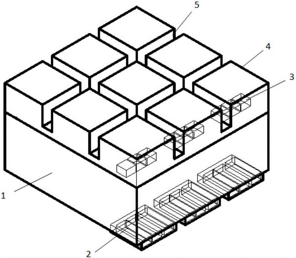
[0046] In this embodiment, combined with figure 1 Be explained:

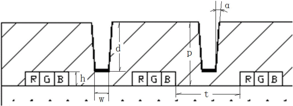
[0047] Dot pitch d=1.5mm, dot matrix arrangement with a resolution of 80*80 integrated LED display packaging module, the display packaging module includes driver IC2, driver circuit board 1, LED lamp module 3, packaging glue 4, driver IC2 welding On the back of the driving circuit board 1, the LED light module 3 is fixed on the front of the driving circuit board 1, wherein the blue and green LED chips have a size of 7 mils*9 mils, and the red LED chip has a size of 6 mils*6 mils. The thickness of the encapsulant 4 is not specifically limited. A groove 5 is provided on the encapsulant 4 between each LED lamp module 3. In this embodiment, the groove 5 is directly molded by molding equipment. The depth d of the groove 5 is not specifically limited, and the depth d is smaller than that of the encapsulant. 4 thickness p and greater than the height h of the LED chip. The width and draft angle of the groove 5 are no...

Embodiment 3

[0051] In this embodiment, combined with figure 1 and image 3 Be explained:

[0052] In this embodiment, the dot pitch d=1.5mm, the dot matrix arrangement with a resolution of 80*80 is integrated into the LED display packaging module, and the display packaging module includes a driver IC2, a driver circuit board 1, an LED lamp module 3, and a packaging glue 4. The driver IC 2 is welded on the back of the driver circuit board 1, and the LED light module 3 is fixed on the front of the driver circuit board 1. The size of the blue and green LED chips is 7mils*9mils, and the size of the red LED chips is 6mils*6mils. The thickness of the display module encapsulant 4 is not specifically limited. A groove 5 is provided on the packaging glue 4 between each LED lamp module 3. In this embodiment, the groove 5 is directly molded by molding equipment. The depth d of the groove 5 is specifically limited, and the depth d is smaller than the packaging glue. 4 thickness p, and greater than...

Embodiment 4

[0055] In this embodiment, combined with figure 1 , image 3 Be explained:

[0056] In this embodiment, the dot pitch d=1.5mm, the dot matrix arrangement with a resolution of 80*80 is integrated into the LED display packaging module, and the display packaging module includes a driver IC2, a driver circuit board 1, an LED lamp module 3, and a packaging glue 4. The drive IC 2 is welded on the back of the drive circuit board 1, and the LED light module 3 is fixed on the front of the drive circuit board 1, where the blue and green LED chip size is 7mils*9mils, and the red LED chip size is 6mils*6mils . The thickness of the display module encapsulant 4 is not specifically limited. Grooves 5 are provided on the encapsulant 4 between the LED lamp modules 3. In this embodiment, the grooves 5 are directly molded by molding equipment, and the depth of the grooves 5 is specifically limited, and the depth d is smaller than the thickness of the encapsulant 4. p, and the thickness of th...


PUM


Abstract

The invention relates to an integrated LED display packaged module and a manufacturing method of the integrated LED display packaged module. A drive IC of the packaged module is welded to the back of a drive circuit board, and LED lamp modules are fixed to the front of the drive circuit board; packaging glue covers the drive circuit board, and grooves are formed in the packaging glue among the LED lamp modules; a micro-nano-scale filler capable of absorbing light rays is uniformly mixed in the packaging glue; the cross sections of the grooves are trapezoid-shaped, and coatings are arranged on the side walls of the grooves. According to the integrated LED display packaged module, the packaging glue is filled with the micro-nano-scale filler being in black or other colors and being capable of absorbing the light rays, therefore, the light flee problem is solved under the premise that certain brightness of an LED screen is consumed, so that the LED display screen has the clear display effect. With the packaged device, the filling and packaging of the packaging glue are realized in the vacuum environment is realized, therefore, the consistency of the packaging glue is effectively realized, the packaging efficiency is promoted, and the yield and the optical effect of the product are improved.

Description

technical field [0001] The invention belongs to the technical field of LED display screens, and relates to an integrated packaging LED display module and a manufacturing method thereof. Background technique [0002] The integrated LED display module includes an LED display module composed of a driver IC, a driver circuit board and red, green and blue primary color LED light-emitting chips. The current common practice is: solder the driver IC on the back of the driver circuit board, place the LED chip upright and fix it on the corresponding pixel position on the front surface of the driver circuit board through an adhesive, and then connect the blue and green LED chips by wire bonding. The positive and negative electrodes and the positive electrode of the red LED crystal unit (single electrode) are connected to the corresponding circuit position of the circuit board by welding the connecting wire (gold wire or aluminum wire), and finally sealed with glue on it for protection....

Claims


Application Information

Patent Timeline
Patent Type & Authority Applications(China)
IPC IPC(8): G09F9/33
CPCG09F9/33
Inventor 程宏斌王瑞光孙天鹏王聪马新峰
Owner CHANGCHUN CEDAR ELECTRONICS TECH CO LTD
Learn More