Packaging structure for film volume acoustic wave filter and packaging method

A thin-film bulk acoustic wave and packaging structure technology, applied in electrical components, impedance networks, etc., can solve the problems of difficult miniaturization of devices, low packaging efficiency, and application impact, and achieve the effect of miniaturization and improved packaging efficiency.

Inactive Publication Date: 2017-01-04
CHINA ELECTRONICS TECH GRP NO 26 RES INST
View PDF6 Cites 8 Cited by
  • Summary
  • Abstract
  • Description
  • Claims
  • Application Information

AI Technical Summary

Problems solved by technology

Although such a packaging structure meets the requirement that the device cannot be polluted, there are at least two disadvantages in the following aspects: 1. It is difficult to miniaturize the device. At present, the smallest ceramic shell is 1.6mmX1.2mm and the thickness is more than 1mm. In the future mobile devices 2. The processing efficiency is low, because each device needs to be processed separately, and there is nitrogen and air replacement in order to keep the chip in a clean and non-polluted environment. Therefore, the packaging efficiency is relatively low

Method used


Image

  • Packaging structure for film volume acoustic wave filter and packaging method
  • Packaging structure for film volume acoustic wave filter and packaging method
  • Packaging structure for film volume acoustic wave filter and packaging method

Examples


Embodiment Construction

[0020] The present invention will be described in detail below in conjunction with the accompanying drawings and specific embodiments.

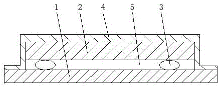
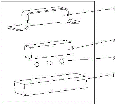
[0021] see figure 1 and image 3 , it can be seen from the figure that the thin film bulk acoustic wave filter packaging structure of the present invention includes a substrate 1 and a chip 2, and corresponding electrodes are arranged on the substrate and the chip, and the chip electrodes are connected by gold balls 3 and the substrate through a flip-chip welding process. The electrodes are connected correspondingly. A film layer 4 is glued and fixed on the surface of the substrate 1 , and the film layer 4 is closely attached to the surface of the substrate 1 and wraps the chip 2 at the same time, forming a vacuum chamber 5 between the chip 2 and the substrate 1 .

[0022] The film bulk acoustic wave filter packaging method of the present invention, the film bulk acoustic wave filter has the aforementioned packaging structure, and the speci...


PUM


Abstract

The invention discloses a packaging structure for a film volume acoustic wave filter and a packaging method. The packaging structure comprises a substrate and a chip, wherein a chip electrode is correspondingly connected with a substrate electrode through flip chip; a film layer is fixedly spliced on the surface of the substrate; the film layer is clung to the surface of the substrate and is wrapped on the chip. The packaging method comprises the following steps: 1) dividing a chip packaging area on the substrate; 2) respectively welding the electrode on the to-be-packaged substrate with the corresponding electrode in the corresponding area through a flip-chip bonding technique; 3) pasting a protecting film on the substrate and wrapping all the chips; 4) raising temperature, splicing and curing the protecting film; 5) cutting the substrate, thereby acquiring the film volume acoustic wave filter. According to the invention, the chips are prevented from being polluted, the microminiaturization is realized and the processing efficiency is increased.

Description

technical field [0001] The invention relates to a film bulk acoustic wave filter (FBAR), in particular to a miniaturized packaging technology for a film bulk acoustic wave filter (FBAR), and belongs to the technical field of acoustic wave filters. Background technique [0002] At present, the miniaturized packaging of film bulk acoustic wave filter (FBAR) adopts the packaging form of potting resin packaging. In the future, there will be higher requirements for miniaturized packaging, and the potting resin is difficult to control the pollution problem. The thin-film bulk acoustic wave filter has high requirements on the working surface and cannot be polluted. Therefore, the packaging form of the potting resin is difficult to meet the needs of actual use. There is also a packaging structure that uses parallel welding of the ceramic shell, that is, a deep cavity structure is made on the shell, the bare chip is bonded in the deep cavity, and the lead wire is electrically conne...

Claims


Application Information

Patent Timeline
Patent Type & Authority Applications(China)
IPC IPC(8): H03H9/05H03H9/17
CPCH03H9/0523H03H9/174
Inventor 金中何西良杨正兵罗旋升
Owner CHINA ELECTRONICS TECH GRP NO 26 RES INST
Why Eureka
Try Eureka