Semiconductor test device

A test device and semiconductor technology, applied in the direction of single semiconductor device test, measurement device, semiconductor/solid-state device test/measurement, etc., can solve the problems of inability to accurately monitor the actual temperature, inability to accurately control the heating temperature, etc., to achieve accurate temperature Effects of adjustment and reliability improvement

Inactive Publication Date: 2007-01-10
PANASONIC CORP
View PDF1 Cites 7 Cited by
  • Summary
  • Abstract
  • Description
  • Claims
  • Application Information

AI Technical Summary

Problems solved by technology

Depending on the layout of the temperature sensor, it is impossible to accurately monitor the actual temperature of the semiconductor wafer when it is subjected to burn-in due to the heat generation of the semiconductor wafer and the thermal resistance of the parts constituting the burn-in treatment device that are in close contact with the semiconductor wafer
Moreover, due to the large distance between the semiconductor wafer and the temperature sensor, the heating temperature cannot be precisely controlled when considering the influence of thermal resistance

Method used


Image

  • Semiconductor test device
  • Semiconductor test device
  • Semiconductor test device

Examples


Embodiment 1

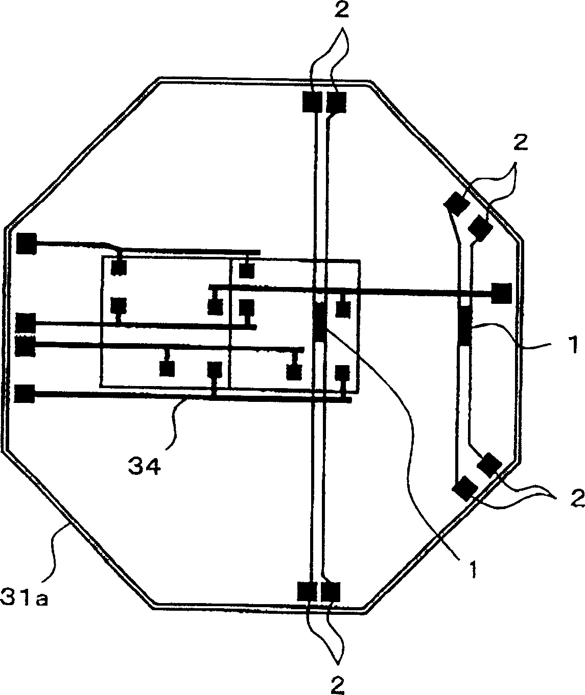
[0057] The preferred embodiment 1 of the present invention relates to the arrangement of temperature sensors. figure 1 This is a bottom view of the semiconductor testing device (detector) according to the preferred embodiment 1. in figure 1 Here, reference numeral 31a denotes a multilayer wiring board. The multilayer wiring substrate 31a corresponds to the multilayer wiring substrate 31 shown in the structure of FIG. 4. Reference numeral 34 denotes a wiring layer of the multilayer wiring substrate 31a. Reference numeral 1 denotes a temperature sensor, and reference numeral 2 denotes a terminal. In the temperature sensor 1, the measurement conditions are set from the outside through at least one of the terminals 2, and the output of the temperature sensor 1 is output to the outside through at least one of the terminals 2 and the output is monitored. The other parts of the structure are similar to the structure in FIG. 4 described above, and will not be described in detail here.

...

Embodiment 2

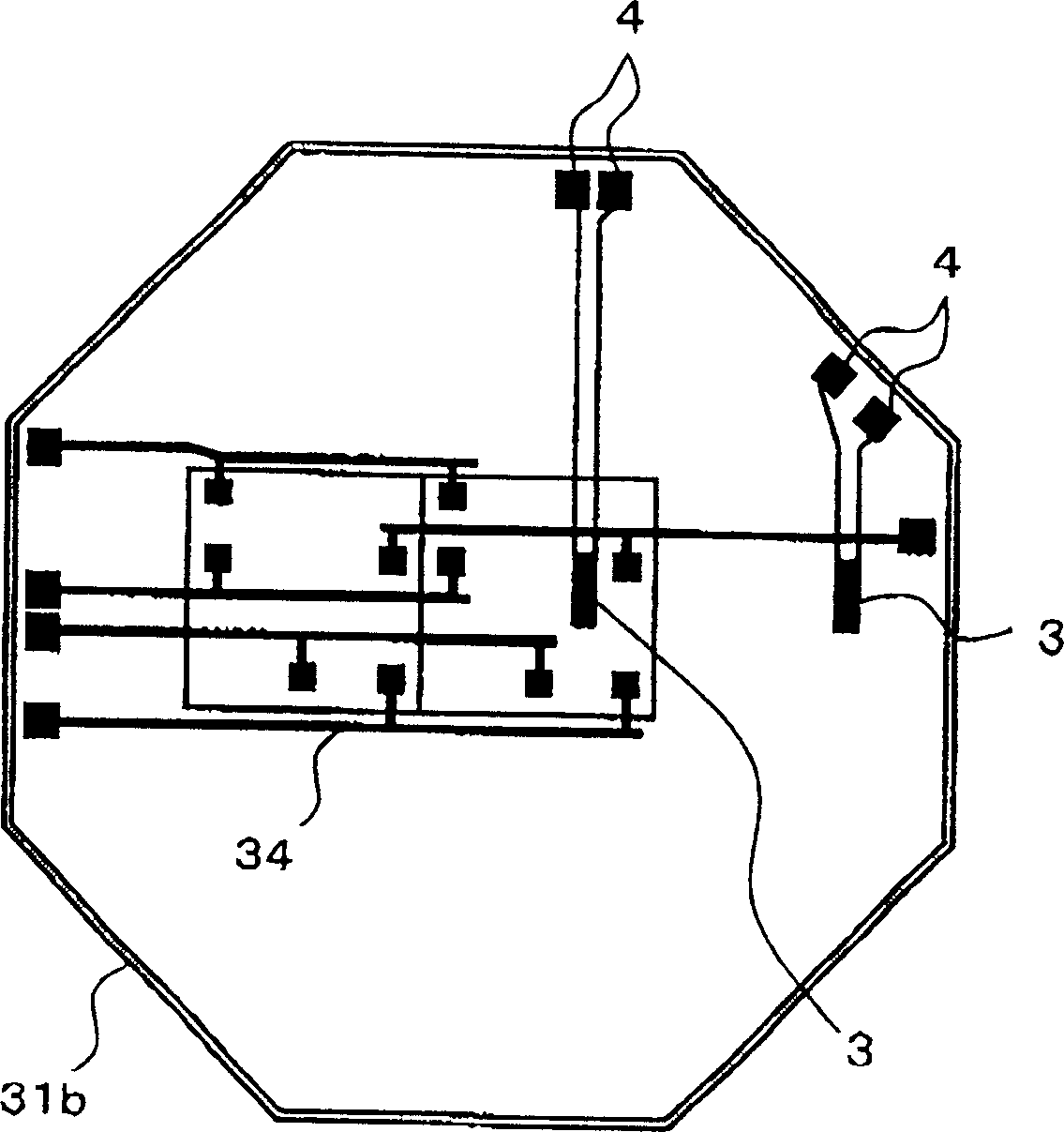
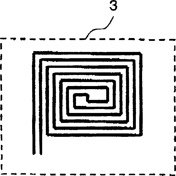
[0072] The preferred embodiment 2 of the present invention relates to the arrangement of the temperature regulator. Figure 2A It is a bottom view of the semiconductor test device according to the preferred embodiment 2. Figure 2B It is a specific example of the temperature regulator 3. Reference numeral 31b denotes a multilayer wiring substrate. The multilayer wiring substrate 31b corresponds to the multilayer wiring substrate 31 in the aforementioned structure of FIG. 4. Reference numeral 34 denotes a wiring layer of the multilayer wiring substrate 31b. Reference numeral 3 denotes a temperature regulator, and reference numeral 4 denotes a terminal. The other parts of the structure are similar to the structure in FIG. 4 described above, and will not be described in detail here.

[0073] The temperature regulator 3 is provided on the surface of the multilayer wiring substrate 31b facing the wafer. The temperature regulating surface of the temperature regulator 3 is flush with the s...

Embodiment 3

[0084] The preferred embodiment 3 of the present invention relates to the arrangement of temperature sensors and temperature regulators. image 3 It is a bottom view of a semiconductor test device combined with a temperature adjustment circuit according to the preferred embodiment 3. in image 3 Here, reference numeral 31c denotes a multilayer wiring board. The multilayer wiring board 31c corresponds to the multilayer wiring board 31 shown in FIG. 4 described above. Reference numeral 34 denotes a wiring layer of the multilayer wiring substrate 31c. Reference numeral 1 denotes a temperature sensor, and reference numeral 3 denotes a temperature regulator. Reference numerals 2 and 4 denote terminals. In the temperature sensor 1, the measurement condition is set from the outside through at least one of the terminals 2, and the output of the temperature sensor 1 is output to the outside through at least one of the terminals and the output is monitored. The temperature regulator 3 is co...


PUM

PropertyMeasurementUnit
temperature coefficient of resistanceaaaaaaaaaa

Abstract

A semiconductor test device comprises a substrate having a opposed-wafer surface on which a semiconductor wafer with a plurality of the embedded semiconductor devices is placing opposite when a burn-in test is implemented, a wiring layer provided on the substrate, and a temperature sensor for measuring a temperature of the semiconductor wafer in the state here the semiconductor wafer is placing opposite on the substrate, wherein the wiring layer includes a wiring which is connected to the semiconductor wafer in the state where the semiconductor wafer is placing opposite on the substrate, and supplies a signal and a voltage for the burn-in test to the semiconductor wafer, and the temperature sensor is provided on the substrate in vicinity of the opposed-wafer surface.

Description

Technical field [0001] The present invention relates to a semiconductor test device, and more specifically, to a bum-in technology in which a collective probe of a semiconductor wafer is used. Background technique [0002] Semiconductor devices and semiconductor wafers are generally subjected to accelerated testing, that is, semiconductor devices and semiconductor wafers must be operated at high temperatures and high voltages in order to detect defective products in advance. Any defects in these defective products will be It was revealed in actual use immediately after the product was manufactured. This test is called "aging". In recent years, the technology of collectively performing burn-in on individual wafers (hereinafter referred to as wafer-level burn-in) described in US Patent No. 5,210,485 has been developed. In wafer-level burn-in, high voltages and signals are respectively input to a power terminal and a plurality of input / output terminals to make each device work. [0...

Claims


Application Information

Patent Timeline
Patent Type & Authority Applications(China)
IPC IPC(8): G01R31/26G01R31/00G01K7/00H01L21/66
CPCG01R31/2874H01L21/67248G01R31/2856
Inventor 三宅直己真田稔
Owner PANASONIC CORP
Why Eureka
Try Eureka