
2.5-dimensional photon crystal-face transmitting laser

A technology for emitting lasers and crystal planes, which is applied in the field of stimulated emission optical devices, and can solve the problems of lasing that cannot achieve zero threshold, increased optical loss, and inability to couple.

Inactive Publication Date: 2007-01-17
INST OF SEMICONDUCTORS - CHINESE ACAD OF SCI
View PDF0 Cites 7 Cited by
  • Summary
  • Abstract
  • Description
  • Claims
  • Application Information

AI Technical Summary

Problems solved by technology

[0004] Two-dimensional photonic crystals have the ability to control the flow of photons in a plane, but they have no effect on photons perpendicular to the plane direction of two-dimensional photonic crystals. Therefore, the photons spontaneously emitted by the active layer region along the vertical direction are directly incident on the air, and cannot Coupled into the lasing mode, which causes an increase in optical loss and cannot achieve zero-threshold lasing

Method used


Image

  • 2.5-dimensional photon crystal-face transmitting laser
  • 2.5-dimensional photon crystal-face transmitting laser

Examples


Embodiment

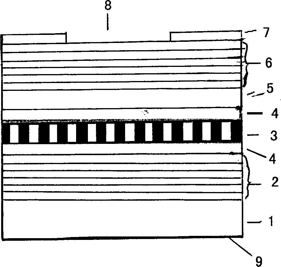
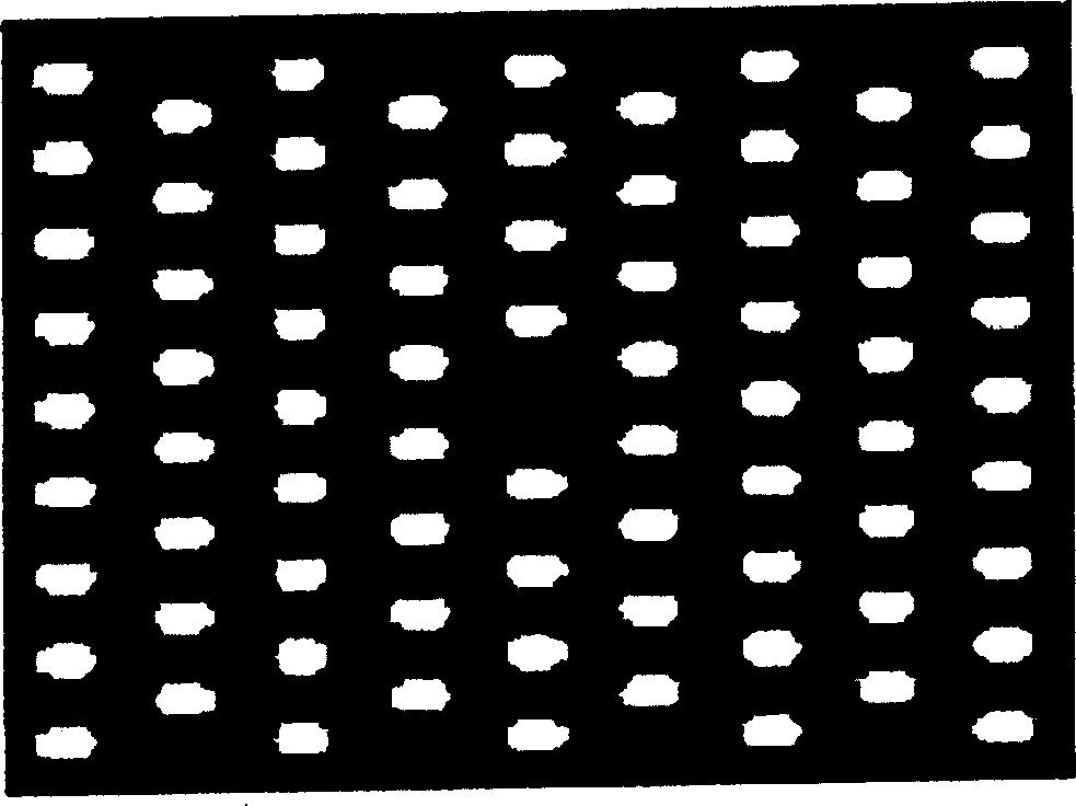
[0034] see again figure 1 As shown, on the n-type GaAs substrate 1, metal oxide chemical vapor deposition (MOCVD) or molecular beam epitaxy (MBE) is used to deposit a multi-layer dielectric high-reflection film with alternating high and low refractive indices, that is, a distributed Bragg mirror (the first DBR layer 2), used as the lower DBR of the laser, the DBR adopts a quarter-wavelength gallium arsenide (GaAs) and aluminum gallium arsenide (AlGaAs) alternately distributed multilayer thin film structure, and the laser is deposited above the first DBR layer 2 The lower cladding layer 4 of the active region, the active layer 3 of the laser is grown on the lower cladding layer 4, and then a planar photonic crystal structure is made on the active layer 3, and defects are contained in the photonic crystal structure, such as figure 2 shown. The photonic crystal structure can be realized by a variety of common photonic crystal manufacturing methods, such as dry etching process r...


PUM


Abstract

A 2.5 Uygur photonic crystal surface emanant laser, including: the wafer; the first DBR layer that is made on the wafer; the below envelope that is made on the first DBR layer; the active layer that is made on the below envelope, and forms the photonic crystal structure on it by the eroding technics; the top envelope that is made on the active layer; the p+ envelope that is made on the top envelope; the second DBR layer that is made on the p+ envelope; the top electrode with the hole that is made on the second DBR layer; the below electrode that is made on the bottom surface of the wafer and covers it.

Description

technical field [0001] The invention relates to a stimulated emission light device, in particular to a stimulated emission light device based on a photonic crystal defect microcavity and made of a 2.5-dimensional photonic crystal. Background technique [0002] Photonic Crystal-PC, also known as Photonic BandGap-PBG material, is formed by the periodic arrangement of materials with different dielectric constants. Similar to the electronic forbidden band in semiconductors, photonic forbidden bands also exist in photonic crystals. Electromagnetic waves within the forbidden band frequency range decay exponentially in photonic crystals and cannot propagate in the crystals. This principle makes it possible to fabricate high-efficiency light emitting devices (light emitting devices-LEDs) and zero-threshold lasers. [0003] Although three-dimensional photonic crystals have the best performance, they are difficult to realize due to the complex process, so current research focuses on ...

Claims


Application Information

Patent Timeline
Patent Type & Authority Applications(China)
IPC IPC(8): H01S5/18H01S5/323
Inventor 陈弘达孙增辉
Owner INST OF SEMICONDUCTORS - CHINESE ACAD OF SCI
Learn More