

Liquid crystal display faceplate with static discharge protection
A liquid crystal display panel, electrostatic discharge protection technology, applied in static indicators and other directions, can solve the problems of limited dispersion of static electricity accumulation in the display area, signal interference, etc., achieve good electrostatic discharge protection function, reduce component damage, and avoid electrostatic discharge the harmful effect of
- Summary
- Abstract
- Description
- Claims
- Application Information
AI Technical Summary
Problems solved by technology
Method used
Image

Examples
Embodiment 1
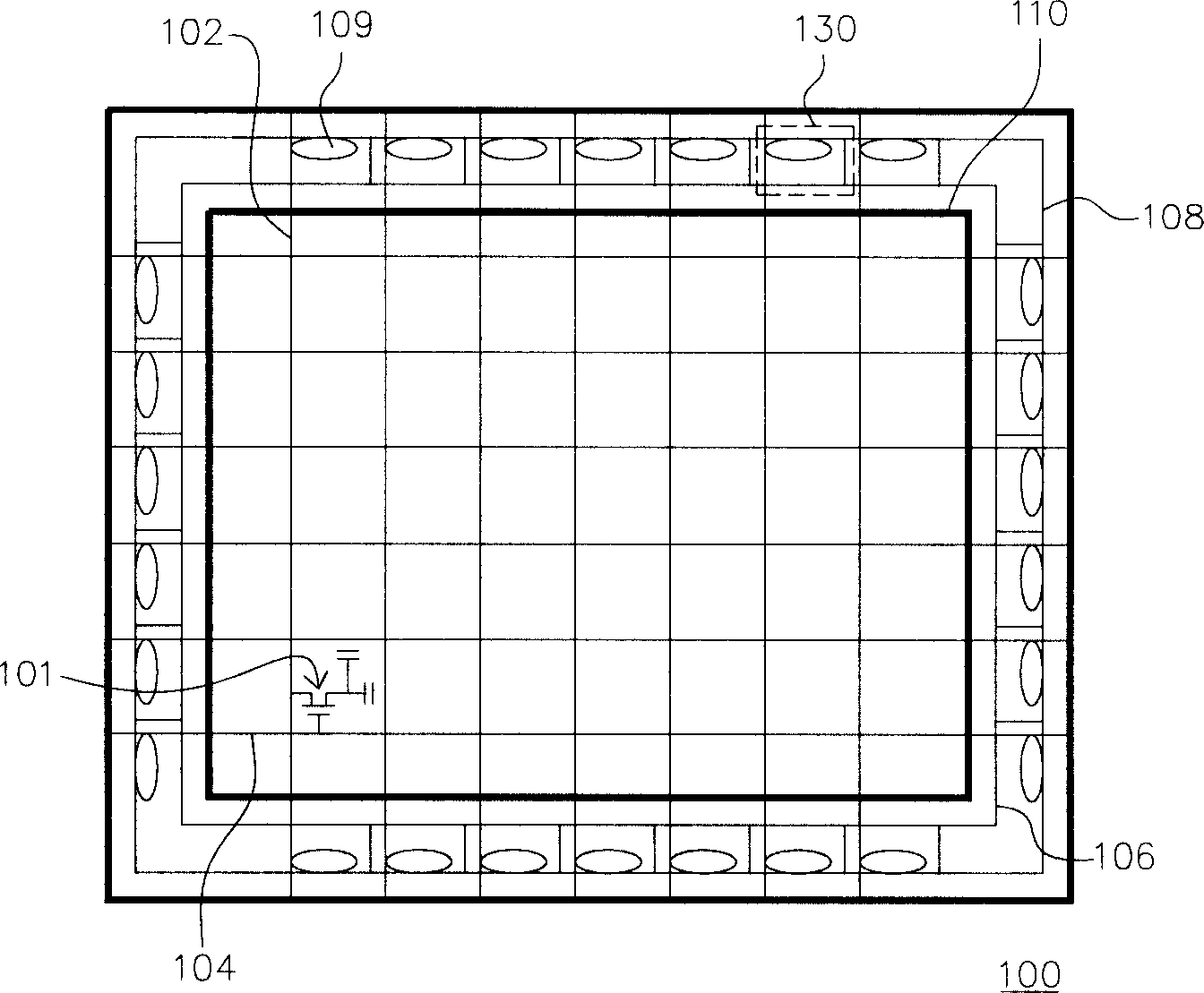
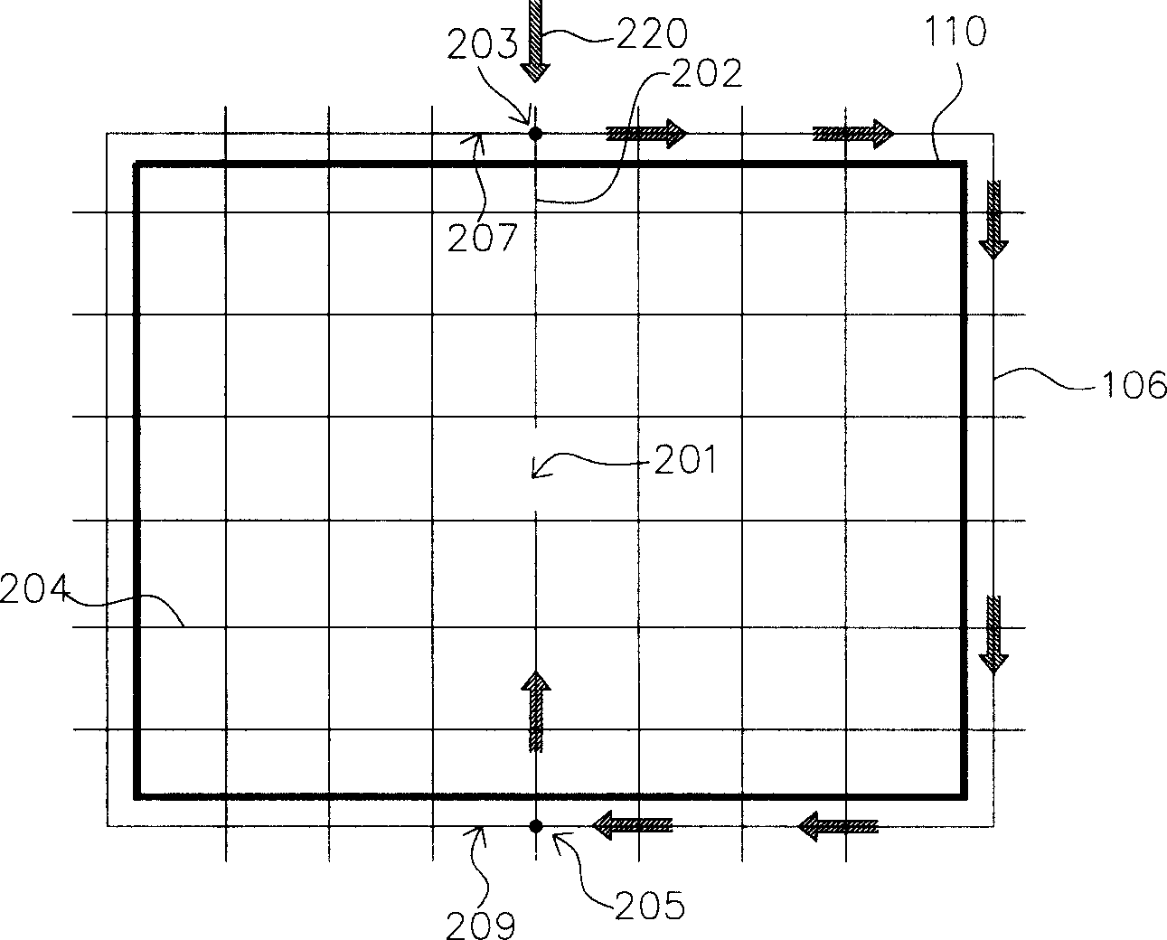
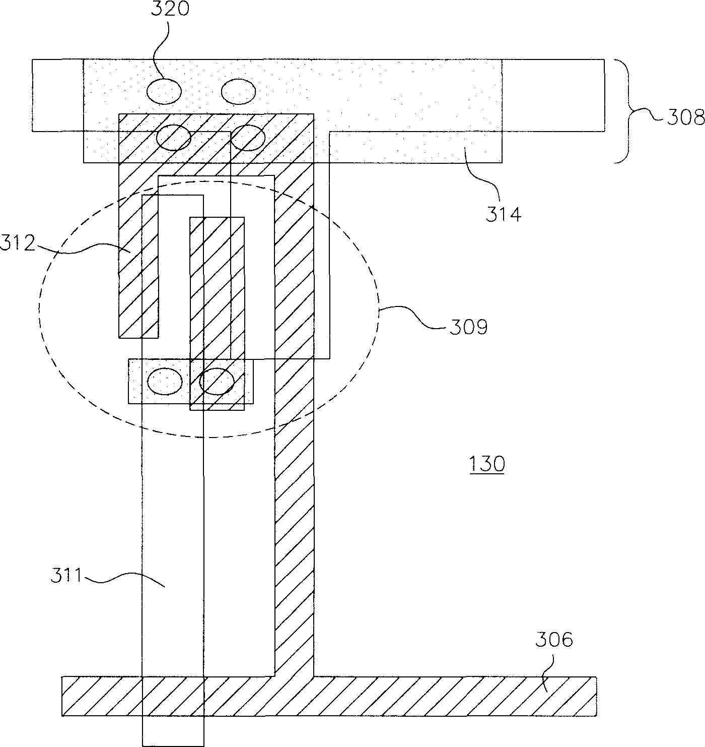
[0038] The invention discloses a liquid crystal display panel circuit structure design with electrostatic discharge protection effect. Reference respectively figure 1 , figure 2 and image 3 , figure 1 It is a schematic plan view of the array structure of the liquid crystal display panel according to the first preferred embodiment of the present invention, figure 2 is a schematic top view of the array structure of the liquid crystal display panel after edge grinding, and image 3 for figure 1 The enlarged schematic diagram of the partial structure of the protection circuit ring of the first preferred embodiment is figure 1 The enlarged schematic diagram within the dashed area 130 in .
[0039] refer to figure 1 , on a liquid crystal display panel 100, the area 110 is a display area with a pixel array, and the data line 102 and the scanning line 104 cross control the switching behavior of each thin film transistor (Thin Film Transistor; TFT) 101 in the display area 110...
Embodiment 2
[0056] The invention discloses another liquid crystal display panel circuit structure design with electrostatic discharge protection effect. Three protective circuit rings are used to set around the display area, while at the same time achieving better electrostatic dispersion effect and disconnection repair function.
[0057] refer to Figure 4 , Figure 4 It is a schematic top view of the array structure of the liquid crystal display panel according to the second preferred embodiment of the present invention. Like the design of the first embodiment, on a liquid crystal display panel 400, the area 410 is a display area with a pixel array, and the data lines 402 It intersects with the scan line 404 to control the display state of each pixel in the display area 410 . In the present invention, three ring-shaped short-circuit protective circuit rings are arranged in the peripheral area outside the display area 410, which are an inner protective circuit ring 406 closer to the pe...
PUM
 Abstract
Description
Claims
Application Information