Electrode transfer film,electrode manufacture method using the film and manufacture method of plasma display panel

A manufacturing method and display panel technology, which are applied in the direction of AC plasma display panels, electrode system manufacturing, discharge tube/lamp manufacturing, etc., can solve the problems of high price and high cost, and achieve the effects of simple process, cost reduction, and waste reduction

Inactive Publication Date: 2007-02-21
LG ELECTRONICS(NANJING) PLASMA CO LTD
View PDF0 Cites 4 Cited by
  • Summary
  • Abstract
  • Description
  • Claims
  • Application Information

AI Technical Summary

Problems solved by technology

This photo etching method (photo etching) needs to use an expensive photo mask, and after exposure, it needs to go through processes such as phase development and sculpture, so the cost is relatively high.

Method used


Image

  • Electrode transfer film,electrode manufacture method using the film and manufacture method of plasma display panel
  • Electrode transfer film,electrode manufacture method using the film and manufacture method of plasma display panel
  • Electrode transfer film,electrode manufacture method using the film and manufacture method of plasma display panel

Examples


Embodiment Construction

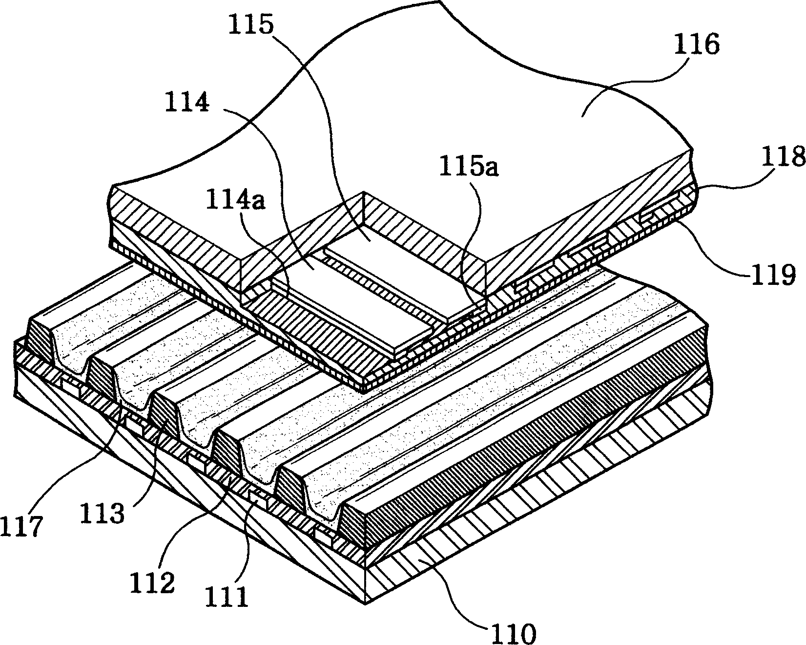
[0033] Hereinafter, preferred embodiments are given, and the plasma display panel of the present invention is described in detail in conjunction with the accompanying drawings.

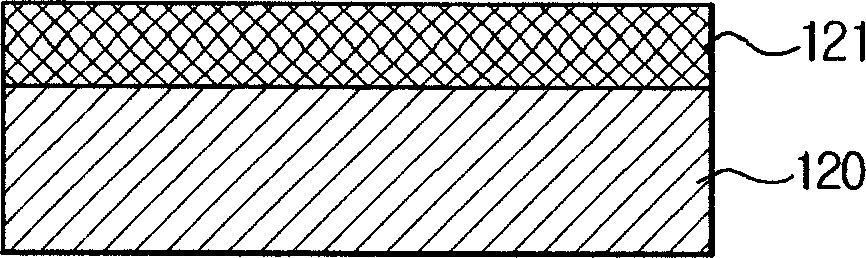
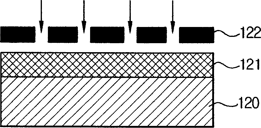
[0034] image 3 It is a sectional view of the electrode transfer film 20 in the embodiment of the present invention. As shown in the figure, it includes: a base film (base film) 21 , a light-to-heat conversion layer 22 formed on the lower end of the above-mentioned base film (base film) 21 , and an electrode material layer 23 formed on the lower end of the above-mentioned light-to-heat conversion layer 22 . Although not shown, a radiation layer may be included between the above-mentioned light-to-heat conversion layer 22 and the electrode material layer 23 .

[0035] The electrode transfer film 20 in the embodiment of the present invention is irradiated with an energy source such as laser light on the part corresponding to the electrode formation circuit, and the irradiated energy source is converted...


PUM


Abstract

The present invention discloses an electrode transfer printing film containing base film, wherein the lower end of the base film forms a light-heat conversion layer and the lower end of the light-heat conversion layer forms a electrode material layer, an electrode manufacture method using the electrode transfer printing film and a manufacture method of plasma display panel. In the present invention, electrodes can be made by a simple procedure using a light source of laser or the like. The procedure is simple without using mask and is capable of reducing the cost of mask; and is adapted to macro-scale and mass production without displaying image procedure, so that the problem of wasting of electrode material is overcome and the cost is reduced.

Description

1. Technical field [0001] The invention relates to an electrode transfer film, an electrode manufacturing method using the electrode transfer film and a plasma display panel manufacturing method. 2. Background technology [0002] A general plasma display panel (PDP: Plasma Display Panel) refers to injecting discharge gas on two substrates forming multiple electrodes, and then negatively applying a discharge voltage. When the gas between the two electrodes emits light, the above discharge voltage generates an appropriate pulse. Voltage, addressed at the point where two electrodes intersect, displays certain numbers, text or diagrams on a flat panel display device. [0003] Such a plasma display panel has a simple process for manufacturing a large panel, has a wide viewing angle, and is of high quality as a self-emitting type. Because of the above-mentioned advantages, it has attracted much attention in the field of flat-panel displays, and is widely used in ultra-thin and la...

Claims


Application Information

Patent Timeline
Patent Type & Authority Applications(China)
IPC IPC(8): H01J9/02B41J2/00B41J2/455H01J11/22H01J11/44
CPCH01J9/02H01J11/12H01J11/22H01J11/24H01J2211/225
Inventor 朴珍旴
Owner LG ELECTRONICS(NANJING) PLASMA CO LTD
Why Eureka
Try Eureka